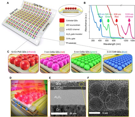
Fig. 1. Schematic of the device structure of the QD/AOS hybrid phototransistor.

(A) A schematic three-dimensional view of a phototransistor array. (B) Optical absorption of QDs used to fabricate the full-color detectors. (C) PbS QDs (10 nm diameter), CdSe QDs (7 nm diameter), CdSe QDs (5 nm diameter), and CdS QDs (3 nm diameter) absorb IR, red, green, and blue, respectively. (D) Three-dimensional impression image of phototransistor and (E and F) corresponding cross-sectional HRTEM images. Scale bars, 50 nm (E) and 5 nm (F). a.u., arbitrary units. Photo credit: Jaehyun Kim, Displays and Devices Research Lab. School of Electrical and Electronics Engineering, Chung-Ang University, Seoul 06974, Korea.
