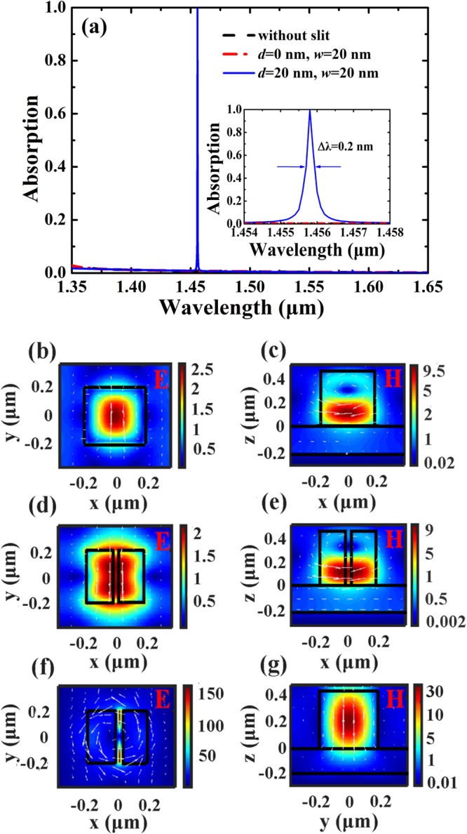
Figure 2.

(a) Absorption response of the SSPs-based metamaterial for the symmetrical (without slit; or d = 0 nm, w = 20 nm) and symmetry-broken (d = 20 nm, w = 20 nm) structures. The inserted figure is the zoomed in view of the absorption response of the symmetry-broken structure. (b) and (c) are normalized electric-field and magnetic-field distributions of the SSPs without slit at the center of silicon patch at 1455.8 nm, respectively. (d) and (e) are normalized electric-field and magnetic-field distributions of the SSPs with d = 0 nm and w = 20 nm at the center of silicon patch at 1455.8 nm, respectively. (f) Normalized electric-field distributions of the symmetry-broken SSPs at the center of silicon patch at 1455.8 nm. (g) Normalized magnetic-field distributions of the symmetry-broken SSPs at the center of slit at 1455.8 nm. White dashed lines and arrows indicate field direction.
