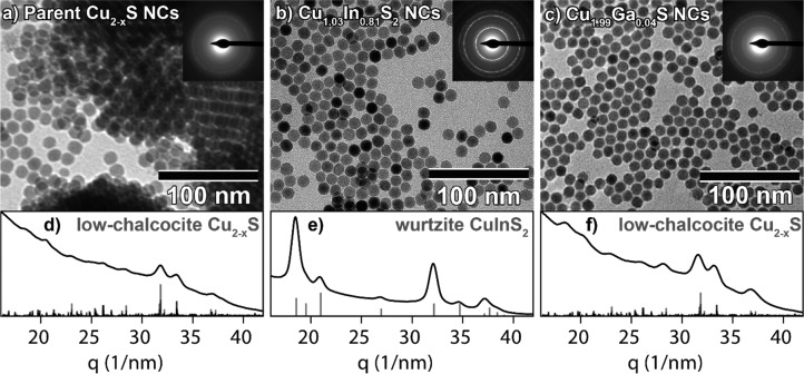
Figure 1.
TEM images of (a) parent Cu2–xS bifrustum NCs, (b) product Cu1.03In0.81S2 (CIS) bifrustum NCs, after reaction with InCl3–TOP at 100 °C, and (c) Cu1.99Ga0.04S nanocrystals, after reaction with GaCl3–TOP at 100 °C. Top-right insets display the corresponding ED pattern. Bottom panels show azimuthally integrated ED (PED) patterns of (d) parent low-chalcocite Cu2–xS nanocrystals, (e) product wurtzite CIS nanocrystals, and (f) product low-chalcocite Cu1.99Ga0.04S nanocrystals. Reference bars in (d,f) are calculated patterns based on the low-chalcocite Cu2–xS crystal structure described in ref (34). Reference bars in (e) were obtained from JCPDS PDF-card 01-077-9459 for wurtzite CIS.

