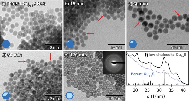
Figure 2.
TEM images of (a) parent Cu2–xS NCs and (b–e) product NCs obtained after reacting the NCs shown in (a) with GaCl3 at 30 °C for (b) 15 min, (c) 30 min, (d) 60 min, and (e) 120 min. Red arrows indicate regions of low contrast within the nanocrystals (cartoons in the lower-left corner give an impression of the observed contrast in the NCs). Top-right inset in (e) depicts an electron diffraction pattern of the corresponding sample. Panel (f) is the azimuthally integrated ED pattern depicted in (e). Reference bars in (f) are calculated patterns based on the low-chalcocite Cu2–xS crystal structure described in ref (34). The blue curve in (f) corresponds to the PED pattern of the parent Cu2–xS nanocrystals. Dotted lines serve as guides for the eye.

