Fig. 2.
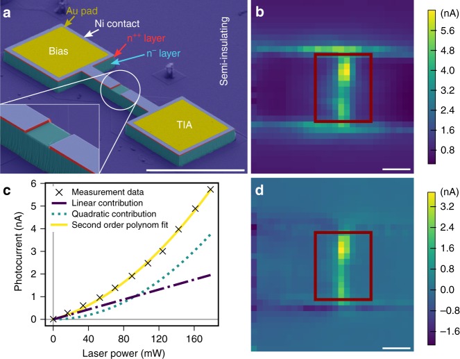
Sample and photocurrent imaging. a SEM picture (functional layers false color coded) of a fabricated device. Bias and transimpedance amplifier (TIA) connections are marked. Inset: Zoom-in of the etched optical opening. Scale bar: 100 µm. b Photocurrent map at −10 V bias. Approximate position of optical access opening marked in red. Scale bar: 5 µm. c Laser power dependence of the photocurrent at the position of maximum two-photon contribution corresponding to a bright spot in panel d. Fit separates linear and quadratic contributions, where stands for optical power. Fit parameters are: = 117.77 6.43 fA mW−2, = 10.96 0.93 pA mW−1. Black crosses denote measurement points, yellow solid line fit . Purple dashed-dotted line shows linear and green dotted line quadratic contribution. d Map of two-photon excitation contribution to photocurrent at maximum laser power obtained via fit parameter . Scale bar: 5 µm.

