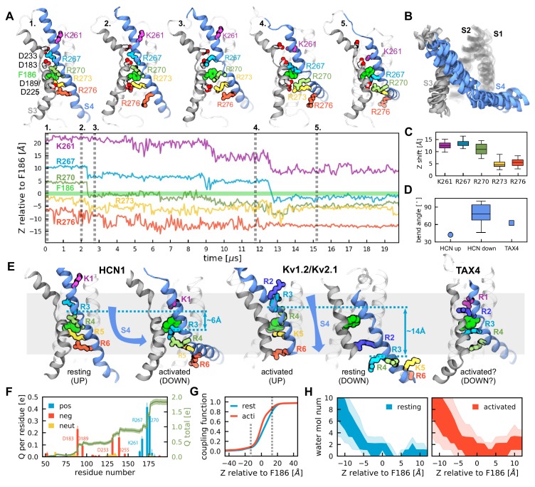
Figure 1. Activation of HCN1 via multi-microsecond long MD simulations.
(A) (Top) Conformational changes of the HCN1 voltage sensor triggered by an applied electric field. Representative snapshots of one voltage sensor along the trajectory are shown. The numbers correspond to the timepoints marked on the trajectory plot below. S4 is shown in blue, S3 in gray, S1 and S2 are transparent. (Bottom) Time-dependent displacement of the gating charges along the membrane normal in a representative voltage sensor measured relative to the charge transfer center (F186). (B) Overlay of representative structures of six activated voltage sensors from two independent ~20 µs simulation runs. (C) Overall displacement of gating charges (S4 basic residues) along the electric field direction. The box plot shows the median, 25-75% (box), 1-99% (bars) of the data collected from the six voltage sensors that underwent activation. (D) A comparison of the bend angles of lower S4 sub-helix with the principal axis of the VSDs of HCN1 and TAX4. HCN1 Up shows the angle between the S4 C-terminus of the HCN1 (PDB 5U6O) and the principal axis of its VSD; HCN1 Down shows the angle between the S4 C-terminus of the simulated structures at the end of the run and the principal axis of its VSD; TAX4 shows the angle between the S4 C-terminus of the TAX4 channel (PDB 5H3O, Li et al., 2017) and the principal axis of its VSD. The box plot shows the median, 25-75% (box), 1-99% (bars) of the data collected from the six voltage sensors that underwent activation. (E) Comparison of the VSDs from the HCN1 activated and resting states, the Kv1.2/2.1 activated and resting state extracted from long timescale simulations (Jensen et al., 2012), and the TAX4 open structure (PDB 5H3O, Li et al., 2017). Small cyan arrows show the displacement of the C atom of R3 along the applied electric field vector. (F) Per-residue gating charge computed per HCN1 subunit. Positive residues are shown in blue, negative in red and non-charged in orange. Green lines show the cumulative gating charge (thick) and the standard error (thin). (G) Coupling function corresponding to the resting (cyan) and activated (red) states. The dashed lines depict the boundaries of the transmembrane part of the voltage sensor. (H) Hydration of the HCN1 voltage sensor in the resting (left) and activated (right) states. The shaded regions show 25-75 (dark) and 10-90 (light) percentiles of the water molecule number collected for the six voltage sensors that underwent activation.


