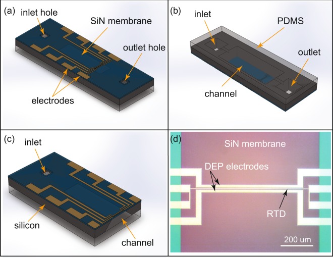
Figure 1.
Device overview. (a) Isometric view of the device. IDEs, RTD, and electrical contacts are integrated on the top surface of the SiN membrane. Inlet/outlet tubing is mounted on the inlet/outlet holes (not shown). IDEs, RTD, and electrical contacts are electrically isolated from the channel by the 500 nm thick SiN membrane. (b) Channel side of the device. Silicon is etched to form the main channel and inlet/outlet with feed through. A 1 mm thick PDMS is placed to complete the channel. (c) Cross-sectional view of the device showing the channel and IDEs/RTD. (d) Close-up optical photograph of the top view of IDEs and RTD on the SiN membrane.

