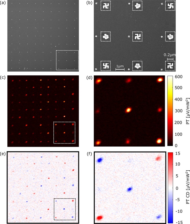
Figure 4.

Chirality-sensitive photothermal imaging. (a) SEM image of a 9 × 9 nanogammadia array. From the 81 nanostructures, 20 are left-handed, 21 are right-handed, and 40 are achiral. The distance between the individual nanostructures is 4 μm in both directions. (b) Higher-resolution SEM image of the bottom right part of the array (the dashed rectangle in (a) shows the area for this image). Detailed images of the structures are shown in the dashed boxes, right of each structure. The scale bars are to show the average distance between two gammadia and the average size of the individual gammadia. (c) Photothermal image of the complete array, displaying the signal of each structure. We normalized the image with the heating power (Ph ∼ 9 mW) and the probe power (Pprobe ∼ 150 μW). (d) Higher-resolution photothermal image of the area shown in (b). (e,f) Photothermal circular dichroism images of the areas in (a) and (b), respectively. We also normalized the images using the heating and probe powers. These images show a clear change of sign in the signal, following the chirality of the nanostructures. As expected, the nominally achiral structures show nearly zero signal. Note that the optical and SEM images cannot be overlapped because they are observed from different sides of the interface.
