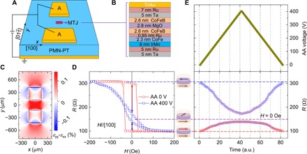
Fig. 1. Voltage manipulation of the MTJ by one pair of electrodes.

(A) Schematic of the experimental setup. One pair of AA electrodes was deposited on the PMN-PT, and an elliptical MTJ device of 18 × 6 μm2 was placed at the center of the gap. Voltage was applied to the AA electrodes to generate localized strain, and the bottom of the substrate was grounded. (B) The detailed structure of the MgO-based MTJ device. To enhance the performance of the devices, we used both the antiferromagnetic layer IrMn and the artificial antiferromagnetic structure of CoFe/Ru/CoFeB. With this particular design, at zero magnetic field, the top CoFeB layer acts as a free layer whose magnetization can be tuned by voltage, whereas the magnetization of the bottom CoFeB layer is fixed because of the pinning effect of the antiferromagnetic IrMn layer. (C) Simulated anisotropic strain distribution upon applying 400 V to the AA electrodes using finite element analysis. A uniform localized tensile strain along the y direction was generated at the central gap of the electrode pair. The dashed-line boxes illustrate the locations of the electrodes. (D) MR curves with 0 and 400 V applied at the AA electrodes. (E) Dependence of resistance on voltage applied to the AA electrodes under H = 0 Oe. The dashed lines denote the various magnetization configurations of the MTJ, as illustrated by the insets, i.e., antiparallel (red), perpendicular (purple), and parallel (blue). a.u., arbitrary units.
