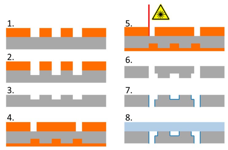
Figure 3.
Schematic illustration of the microfabrication steps for a Si/glass DLD array. The steps are: 1. Photolithographic structuring of the resist for micropost arrays and connection channels; 2. Dry etching of silicon (Bosch Process); 3. Stripping of the resist; 4. Filling of the arrays with resist, structuring the resist for fluidic vias; 5. Fs-laser cutting of the vias; 6. Stripping the resist; 7. Deposition of 200 nm oxide layer; 8. Anodic bonding of glass and silicon.

