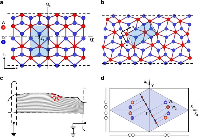
Fig. 3. Symmetry analysis of edges along different directions of WTe2.
a and b Schematic of lattice structures with edges along <100> (a) and <110> (b) directions respectively. The unit cell is shadowed in a blue rectangular in each Figure. The mirror plane Ma of the <100> direction is marked by solid line and the glide mirror plane Mb of the <010> direction is marked by dash line in Figure a, the screw axis along the <001> direction is marked by symbol 21. c Collection of the local photocurrent from a WTe2 device in a Shockley-Ramo-type scheme. The solid gray lines are the weighting field lines of the device used in Fig. 2a with the source contact set at 1 V and the drain contact set at 0 V. The red arrows represent the possible directions of local edge photocurrent. The simulations are performed using COMSOL. d The distribution of Weyl nodes in bulk WTe2 and the projections of Weyl nodes on (100), (010) and (110) surfaces. WTe2 has eight Weyl nodes all locating in kc = 0 plane, each four symmetry-related nodes are referred as W1 and W2 respectively. The mirror symmetry-related Weyl nodes with opposite chirality annihilate in pairs when projected onto (100) and (010) surfaces, but the Fermi arcs can survive in higher Miller-index surface BZs.

