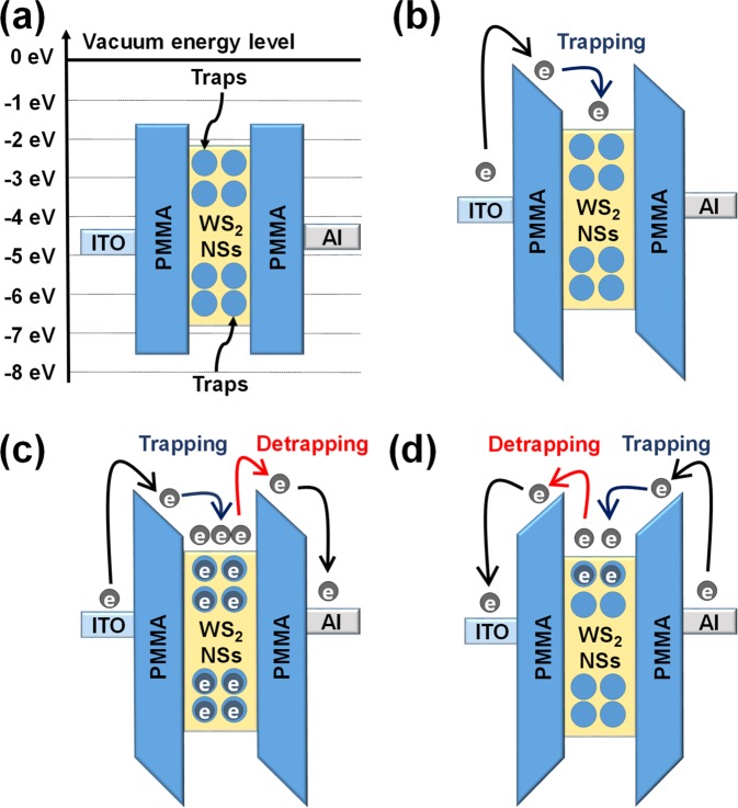
Figure 5.
(a) Schematic diagram of the energy-level bands for the WS2 NSs:PMMA/ITO/PEN memristive device without applied bias. Schematic diagrams of the carrier transport mechanisms in the LRS writing processes when (b) a low bias voltage (0–0.8 V) and (c) a high bias voltage (0.8–2.5 V) are applied. (d) Schematic diagram of the carrier transport mechanisms in the HRS erasing process. The work functions of the ITO film and the Al electrode are −4.8 and −4.3 eV, respectively. The highest occupied molecular orbital level of PMMA is −7.8 eV, and the lowest unoccupied molecular orbital level is −1.8 eV.

