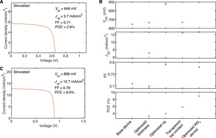
Fig. 6. Simulated performance of optimized devices.

(A) Simulated I-V characteristics of the device geometry used in our experiments, assuming no external series/shunt resistances. (B) Simulated VOC, JSC, fill factor (FF), and power conversion efficiency (PCE) for optimized devices. Apart from the final device geometry (“Optimized WS2 device”), optimizations are independent, not cumulative. (C) Simulated I-V characteristics of the fully optimized WS2 device.
