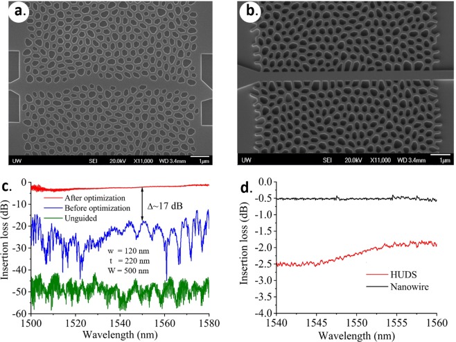
Figure 3.
(a) SEM image of a fabricated SOI HUD waveguide by simply skipping a row of etched air holes. (b) SEM image of a fabricated SOI HUD waveguide (including design optimization). (c) Experimentally measured transmission spectrum comparing performance of HUD waveguide before (a) and after (b) design optimization shows a 17 dB improvement. A flat transmission spectrum across a large range was achieved after waveguide optimization. (d) Experimentally measured transmission spectrum comparing the coupling losses of the optimized HUD waveguide and a silicon strip waveguide. Insertion losses of ~2–3 dB were obtained due to the input/output coupling loss between HUD waveguide and the rest of the devices. Here, w represents the uniform width of the network walls, t is the waveguide thickness (height), and W is the average cell separation and also the fixed width of the waveguide channel in (b). The label ‘unguided’ in Fig. 3(c) refers to the HUDS structure without a waveguide channel embedded in it.

