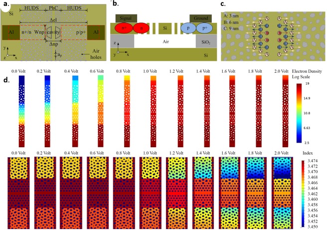
Figure 5.
(a) A schematic of resonant modulators clad with HUDS in p+pinn+ configuration. The top view illustrates waveguide-coupled cavity clad with HUDS, and positions of doping regions. (b) Side view of the device illustrating approximate distributions of p (Boron) and n (Phosphorus) dopants. (c) HUDS resonant cavity design. (d) Top: Pseudo-color display of simulated electron density (log scale in C·cm−3) and bottom: the pseudo-color display of simulated index of refraction distribution (linear scale) for the p+pinn+ device as a function of the magnitude of the applied voltage.

