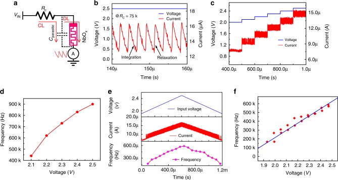
Fig. 3. Characteristics of the artificial spiking afferent nerve (ASAN).
a Schematic of the ASAN. A resistor Rc (75 kΩ) and a NbOx memristor with parallel parasitic capacitance are combined together (RHRS >> Rc >> RLRS). In real applications, the voltage on NbOx top electrode serves as the output spiking signal. The parasitic capacitor (Cparasitic) is tested to be about 20 pF. b The oscillation behavior of the ASAN. For the sake of simplicity, the current flowing through the memristor is measured as the response. The charging time from VH to VTH is defined as the integration time and the discharging time from VTH to VH as the relaxation time. c ASAN response under different input voltages. d Extracted mean value of spiking frequency vs. voltage in c. e Frequency response of the ASAN with triangular stimuli pulses. f The quasi-linear frequency–voltage curve extracted from e.

