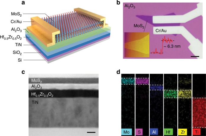
Fig. 1. Schematic of device structure and microscopic representation.
a Structure schematic of MoS2 phototransistors with the ferroelectric HZO thin film in the gate dielectric stack. b Optical microscope photograph of the device with MoS2 channel length of 3 μm, width of 15 μm. Scale bar, 5 μm. The inset is the atomic force microscope (AFM) imaging of the multilayer MoS2 flake, and the thickness of MoS2 is measured as 6.3 nm (9 layers). c Transmission electron microscopy (TEM) imaging of the channel and gate of the device is in order with MoS2/Al2O3/HZO/TiN layers. Interfaces of all layers are clear and flat. Scale bar, 10 nm. d Energy dispersive X-ray spectroscopy (EDS) elemental mapping of Mo, S, Al, Hf, Zr and Ti, corresponding to MoS2/Al2O3/HZO/TiN layers in the TEM imaging.

