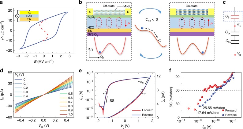
Fig. 2. Electrical measurement and results of the NC MoS2 phototransistors.
a Hysteresis loop (solid blue line) of the 10 nm-thick ferroelectric HZO thin film is measured by a capacitor composed of Au/HZO/TiN layers. The dashed red line fitted by the Landau–Khalatnikov (LK) equation E = 2αP + 4βP3 + 6γP5 shows negative dP/dE region. b Device working schematics and ferroelectric double well energy landscapes. During the process of ferroelectric polarization switching, the ferroelectric material is supposed to go across an energy barrier from one energy valley to another. This energy barrier is regarded as the ferroelectric NC region. c Equivalent capacitance schematic of the device, where CS, Cox and CFe represent the capacitance of MoS2, Al2O3 and HZO layers, respectively. d Output characteristic (Vds–Ids) curves exhibit ohmic characteristics for all gate voltages. e Forward and reverse transfer characteristic (Vg–Ids) curves under Vds = 0.1 V are plotted in red and blue, respectively, and hysteresis between them is almost negligible. Electron mobility and SS are, respectively, extracted based on a linear scale (right axis) and a logarithmic scale (left axis). f SS is calculated according to the transfer characteristic curves, where the average value, the minimum values in forward and reverse (SSavg, SSmin-for, and SSmin-rev) are 45, 17.64, and 25.55 mV/dec, respectively.

