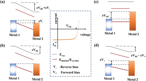
Figure 2.

Metal–Insulator–Metal picture of the thin film device and schematic J–V curves of the solar cells with characteristics of short‐circuit current, V OC. The schematic the division of different work conditions, including a) reverse bias condition: the electric field is bigger than the build in voltage (V BI), b) short circuit condition: the photogenerated charges drift toward the contacts by the V BI, c) open circuit condition: the photogenerated charges recombine and the current becomes zero, and d) forward bias less than V OC: the internal field is weakened by the forward bias. Adapted with permission.53 Copyright 2004, Materials Research Society.
