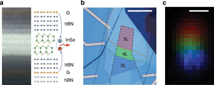
Fig. 1. InSe tunneling devices.
a Cross-sectional annular dark-field scanning transmission electron image of a typical LED device with matching layer schematic on the right. b Optical micrograph of a device used to study resonant tunneling through InSe subbands. Graphene is outlined in black, 2 layer thick (2L) InSe in blue, 4L in green and 5L in red. c Artificially colored electroluminescence (EL) map of the device shown in b: blue corresponding to EL around 1.98 eV, green 1.50 eV and red 1.35 eV with sampling bandwidth of 1 meV (detailed EL spectra can be found in SI). The scale bars are .

