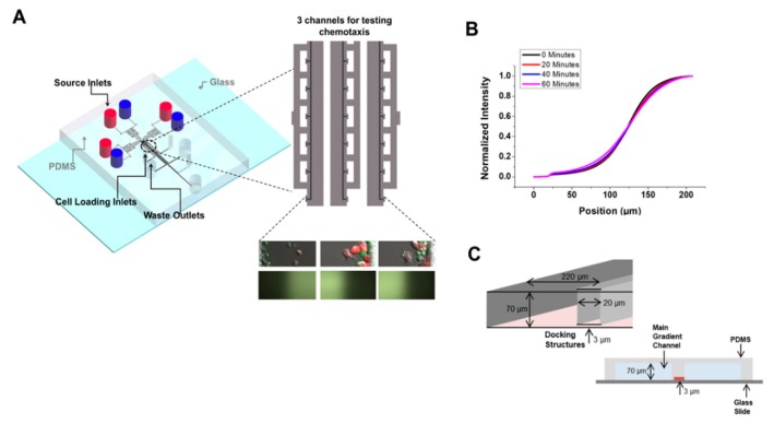
Figure 1.
Device schematic and gradient profile calibration of the D3-Chip. (A) A schematic illustration and gradient profile using FITC-dextran of the D3-Chip; (B) The gradient profile of the D3-Chip for 60 min, indicated by one of the gradient generating channels as a representation; (C) Illustration of the cell docking structure. Cells would dock at the barrier and change their morphologies to squeeze and migrate under the ~3 µm gap into the main gradient channel. A 2D cross section view also is visualized to show the docking area and the main gradient area, separated by the docking structure with only the ~3 µm gap to connect the two sections.

