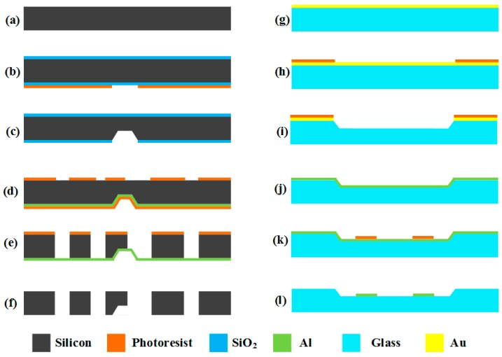
Figure 11.
Fabrication process of the silicon structure and glass electrode substrate: (a) The processing of the structure starts with a double polished silicon wafer. (b) After high-temperature thermal oxidation, a layer of SiO2 is grown on the silicon wafer, and then photolithography and development processes are done on the back side of the silicon wafer. Part of the photoresistant layer is removed to prepare for the wet etching in the next step. (c) After removing part of SiO2, the remaining SiO2 is used as a new mask, and then the wet etching process is conducted on the silicon wafer. (d) Firstly, the SiO2 on both sides is removed, and a layer of aluminum is sputtered on the back side of the silicon wafer as the cut-off layer. Then, a layer of photoresistant layer is used to protect the aluminum from the corrosion of the developer. At last, the second photolithography and development processes are done on the front side of the silicon wafer. Part of photoresistant layer is removed to prepare for the dry etching in the next step. (e) After removing the photoresistant protective layer on the back, dry etching is done on the front side continuously until the whole silicon wafer is etched to the cut-off layer. (f) Removing all of the photoresistant layer and the aluminum, the structure processing is completed. (g) The processing of the electrode substrate starts with a glass wafer, and a layer of gold is evaporated on the front of the glass wafer. (h) The photolithography and development processes are done on the gold layer, and part of photoresistant layer is removed. (i) After removing part of the Au, the remaining Au serves as the mask, and wet etching is done on the glass wafer to make the gaps and provide the motion space for the silicon structure (c). (j,k) After removing all of the photoresistant layer and the Au, a layer of aluminum is sputtered on the gap. Then, the photolithography and development processes are done on the aluminum layer. Part of photoresistant layer is then removed, and the rest of the photoresistant layer serves as the mask to prepare for the next step. (l) After removing the aluminum without mask layer protection, the mask layer is removed and the electrode substrate is finished.

