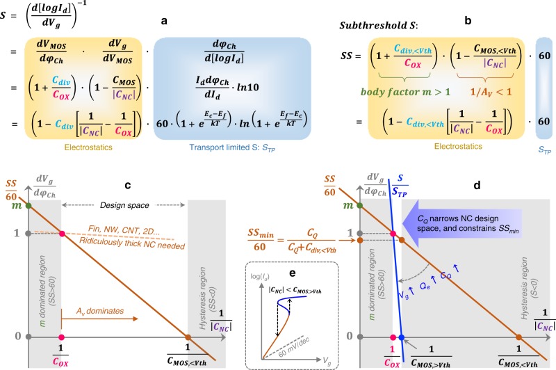
Fig. 2. Impact of electrostatics and quantum capacitance on NC-FET design space.
a Formulating Id-Vg slope or swing (S) by decoupling the electrostatics and transport contributions. STP is the transport limited S. b S is reduced to subthreshold S (SS) in the subthreshold regime. STP is reduced to 60 mV per decade. Body factor m (>1) and voltage gain AV (>1) compete with each other in determining SS. c Visualizing the SS formula and its physics. In the shaded region on the LHS, m dominates, thus SS > 60 mV per decade. In the shaded region on the RHS, SS < 0, represents the appearance of hysteresis. The design space here is between the two shaded regions where AV dominates and 0 < SS < 60. The dashed line illustrates the ultra-small negative slope of SS/60 line (which implies that SS/60 can be noticeably below 1 only for 1/|CNC| ≫ 1/Cox) for Fin-, nanowire (NW)-, carbon nanotube (CNT)- and 2D- FETs, indicating very small |CNC|, or equivalently very thick NC layer in these devices is required to obtain NC benefit. d A picture that captures all essential quasi-static device physics of NC-FETs. Note that in the near and above-threshold region, the SS/60 line transforms to the S/STP line, which rotates clockwise due to the rapidly increasing quantum-capacitance CQ with gate bias till a nearly vertical position is reached when the device is fully turned on. Since S in the entire range of Id–Vg curve should be guaranteed to be positive, in order to prevent hysteresis in both sub- and super- threshold regimes, the lower bound of 1/|CNC| is extended to 1/CMOS,>Vth, leading to a narrow NC design space and a minimum hysteresis-free SS ( = CQ/(CQ + Cdiv,<Vth)) at 1/|CNC| = 1/CMOS,>Vth. e Id-Vg curve of an example NC-FET in which 1/|CNC| is designed to be within the shaded region on the RHS of (d). Although SS (brown colored portion) is small, negative S (i.e., hysteresis) appears in the near- or above-threshold region (blue colored portion).

