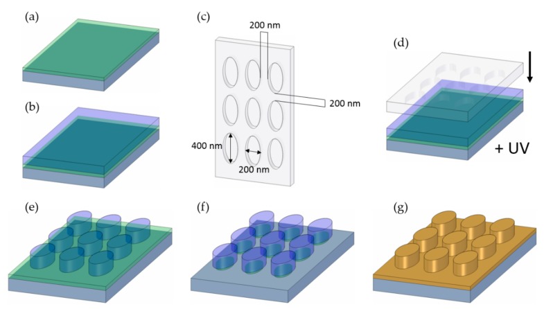
Figure 1.
Schematic nanostructure fabrication (not to scale): (a) deposition of the lift-off resist (green) on top of a silicon substrate; (b) deposition of the imprint resist (blue); (c) employed stamp with elliptical holes separated by a gap of 200 nm as indicated and elliptical holes with a major axis of 400 nm and a minor axis of 200 nm; (d) actual imprint process of the imprint resist by pressing the stamp into the resist, followed by curing the resist by ultraviolet (UV)-light exposure; (e) imprinted structure in the resist after removal of the stamp with a pillar height corresponding to the imprint resist thickness of 200 nm; (f) final imprint structure after reactive ion etching and wet-chemical etching, resulting in an undercut etch of the lift-off resist; (g) deposition of a Au layer of 50 nm thickness to obtain the final metal nanostructure.

