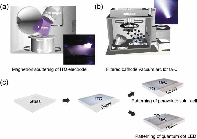
Figure 1.

(a) Schematic of the DC magnetron sputtering system employed for deposition of the ITO anode on glass substrates at room temperature. Schematic of the ITO sputtering plasma FCVA process for coating of ta-C layers with different thicknesses on the ITO anode. The inset shows the arc plasma beam. (c) Schematic fabrication process of the patterned ta-C/ITO anode for PSC and QDLED devices.
