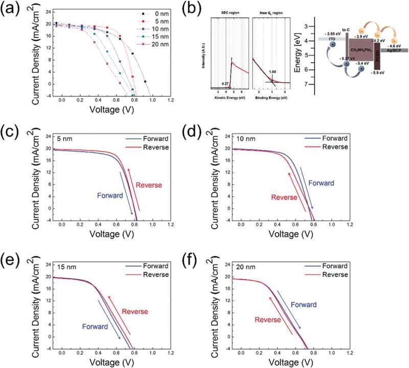
Figure 6.

(a) Current density–voltage (J-V) curves of PSCs fabricated on the ta-C/ITO anodes with increasing ta-C thickness. (b) UPS spectrum used to determine the work function and valence band maximum (VBM) of the ta-C film and the energy band diagram of the PSCs. Current density–voltage (J-V) curves for forward and reverse scans (74 mV/s) of the solar cell with different ta-C thicknesses – (c) 5 nm, (d) 10 nm, (e) 15 nm, (f) 20 nm.
