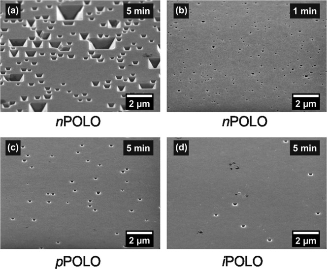
Figure 7.

SEM images of full area reference samples on 80 Ω cm p-type wafers after etching with 15% TMAH at 80 °C. The samples are tilted 31° out of the vertical position. In image (a) after etching for 5 min the etch pit are so wide that they are growing into one another, which would falsify the areal density. Thus, we chose a shorter etching time of 1 min (b) for the evaluation of this sample. In image (c,d) the etching time of 5 min is appropriate for determining the pinhole areal density.
