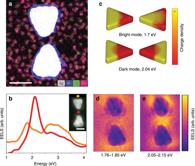
Fig. 1. Plasmonic bowties coupled with quantum dots.
a Electron micrograph of a plasmonic bowtie with QDs in its vicinity. The image is a color-coded superposition of elemental maps taken by EDS in the STEM. The color key is shown at the bottom of the image. The scale bar represents 50 nm. b EEL spectra of a bare bowtie measured at the two locations indicated by matching colored dots in the inset, which is an annular dark-field (ADF) STEM image of the device. The scale bar represents 50 nm. c Simulated charge-density maps for the bright and dark dipolar modes at the indicated energies. d, e Experimental EEL maps for the bright (d) and dark (e) modes, constructed at the indicated energy ranges.

