Fig. 2.
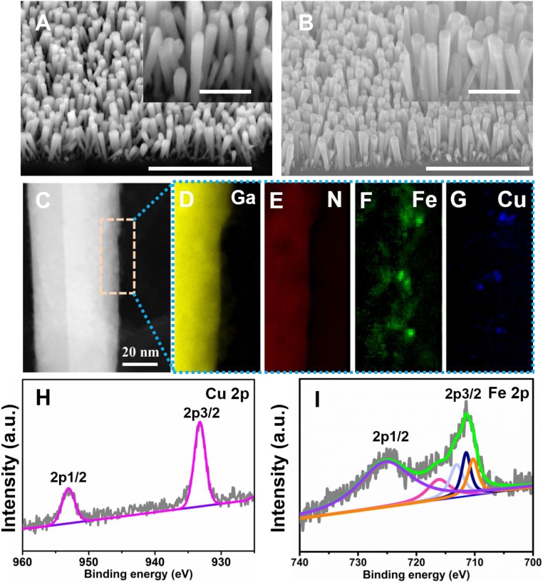
Structure and chemical characterization. Scanning electron microscopy (SEM) images of bare GaN NWs/Si (A) and CuFe@GaN NWs/Si (B) with magnified Insets. (Scale bars: A and B, 1 μm; Insets, 500 nm.) STEM-HAADF image of GaN nanowire NW modified with binary CuFe catalyst (C). The elemental distribution mappings of Ga (D), N (E), Fe, (F) and Cu (G) are described as well; the full horizontal width of D–G is 20 nm. XPS measurement of Cu 2p (H) and Fe 2p (I) in CuFe@GaN NWs/Si. a.u. denotes arbitrary unit; in H, the gray and pink lines represent original and fitting data of Cu 2p, respectively; in I, the gray and green lines represent original and fitting data of Fe 2p while orange, deep blue, light blue, pink, and purple lines represent various iron oxides and/or hydroxides.

