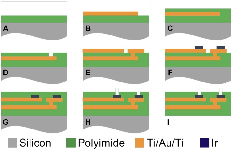
Fig. 3.
Cross-sectional view of the microfabrication process for electrode arrays. A: deposition of 5-µm Polyimide 1 layer (green) atop a silicon wafer substrate (gray). B: deposition and patterning of trace metal 1 (Ti/Au/Ti). C: polyimide 2 deposition (2 µm). D: interconnection via etching (achieve using O2 plasma). E: deposition and patterning of trace metal 2 (Ti/Au/Ti). F: deposition and patterning of Ir electrode metal. G: polyimide 3 deposition (5 µm). H: electrode via etching. I: device outline etching. Images are not drawn to scale and adapted with permission from Tooker et al. 2012).

