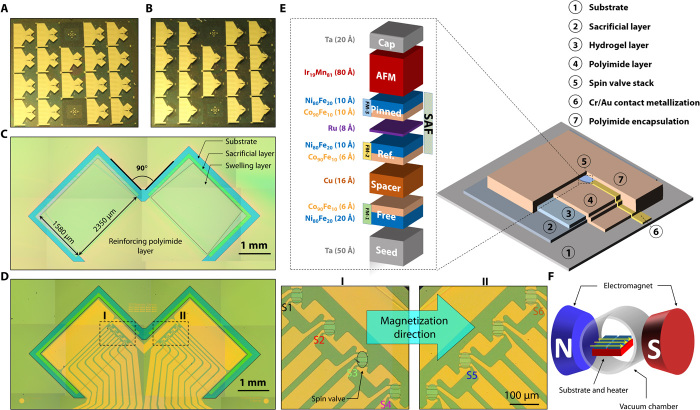
Fig. 2. Wafer-scale fabrication of 3D vector field encoder manufactured on 50 mm by 50 mm square glass substrates and their magnetoelectrical characteristics in the planar state.
(A) Initial planar devices. (B) Wafer-scale self-assembled devices. (C) Fabricated planar shapeable polymeric stack. (D) Schematic that shows the exact SV stack. (E) Simplified scheme of the complete layer stack involving shapeable polymer platform, sensor elements, contact metallization, and encapsulation layer. The SV ellipses are patterned and then electrically connected with Cr/Au electrodes and protected by a thin PI layer. (F) Schematic that depicts vacuum oven magnetization setup magnetizing SVs at 300°C for 1 hour with a superimposed magnetic field of ~700 mT produced by an electromagnet. Photo credit: Daniil Karnaushenko, Institute for Integrative Nanosciences, Leibniz IFW Dresden.

