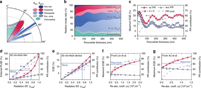
Fig. 3. PeLED analysis using TMF modelling.
a Angular mode analysis for PeLED with a structure of glass/ITO (150 nm)/PVK (10 nm)/PEA2Csn−1PbnBr3n+1 perovskite (50 nm)/TPBi (50 nm)/LiF (1 nm)/Al. Proportions of active absorption (Aact) and parasitic absorption (Apara) for each mode are represented by unique colours in a–b. b Relative ratios of each mode in PeLED for various perovskite thickness. c–g Calculated EQEs (of PL or EL) with PR (closed red circles), without PR (closed grey squares) and without re-absorption (open navy squares), as well as relative PR contribution (violet dashed lines) for c an ideal PeLED (IQE = 100%) with various perovskite thickness; d a 50 nm-thick perovskite film on glass; e a PeLED with 50 nm-thick perovskite (ηinj = 100%); and f–g, the PeLED structures reported by Lin et al.4 and Xu et al.5, respectively, with 100% IQE. For d–g the blue dashed lines compare the graphs with the experimentally measured or reported values. The fact that the calculated ηrad (75%) of the PeLED e is almost the same as that of the neat film d indicates that the assumption of ηinj = 100% is a good approximation, at least for the voltage of 2.6 V where the maximum EQE occurs. See Supplementary Figs. 10–12 for further details.

