
Fig. 3. Optical simulation.
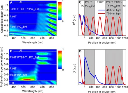
(A) Simulated optical field distribution and (B) the normalized photogenerated electron distribution across the 300-nm-thick binary blend P3HT:PC70BM (100:1) visible light–absorbing layer, 320-nm-thick pristine P3HT optical spacer layer, and 500-nm-thick ternary blend P3HT:PTB7-Th:PC70BM (70:30:1) NIR light–absorbing layer in the dual-mode OPD. (C) Optical field distribution and (D) profile of the photogenerated charge carriers calculated for the dual-mode OPD at two different wavelengths of 460 and 770 nm.