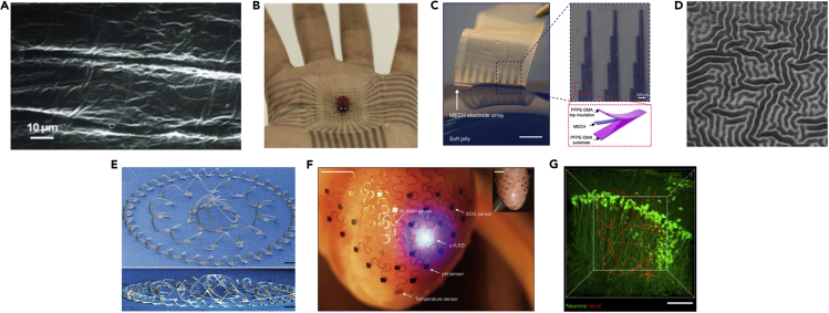
Figure 3.
Flexible Electronics
(A) Scanning electron micrograph of a polypyrrole film, containing the dopant p-toluenesulfonate anion deposited on a gold layer over a PDMS substrate.
(B) A photograph of an intrinsically stretchable transistor array adhering and conforming to a human palm.
(C) A multielectrode array based on a hydrogel prepared by photolithography, showing good control over electrode placement and size. Scale bar, 2 mm and 200 μm (insert).
(D) Optical image of a 100-nm-thick gold layer deposited on a PDMS substrate after strain has been relieved from the substrate. Scale bar, 100 μm.
(E) SEM image of a complex 3D mesostructure formed from a 2D precursor that consists of closed-loop circular filamentary serpentines and radially oriented ribbons, selectively bonded to a biaxially stretched elastomer substrate. Scale bar, 400 μm.
(F) Image of a flexible device consisting of serpentine filaments integrated on a Langendorff-perfused rabbit heart. The white arrows highlight various function elements in this system. Scale bar, 6 mm.
(G) 3D interface between an ultra-flexible device with neuron-size features (red) and neurons (green). Scale bar, 100 μm. Reproduced with permission from Wang et al., 2011, Wang et al., 2018, Liu et al., 2019, Xu et al., 2014, Xu et al., 2015, Yang et al., 2019; and Lacour et al., 2003.

