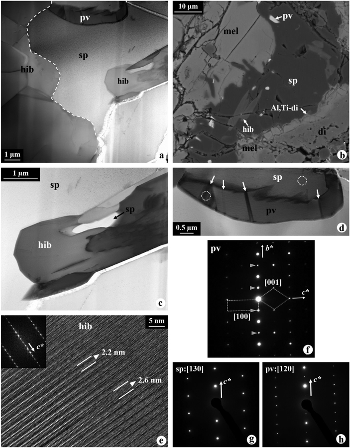
Figure 4.
(a) BF STEM image of highly curved hibonite-spinel interface, as outlined by the dotted line. (b) BSE image of platy spinel at the interface with the CAI mantle. (c) BF STEM image of defect-structured hibonite inclusion in spinel that contains elongated spinel. (d) BF STEM image of elongated perovskite surrounded by spinel. The twinning planes in perovskite, indicated by arrows, are apparent. (e) HR TEM image of hibonite that consists of irregular intergrowths of 2.6 nm (001) spacing within 2.2 nm (001) spacing. The inset Fast Fourier Transform patterns, indexed as the [] zone axis, show strong streaking along c*, consistent with the presence of stacking defects. (f) Electron diffraction patterns of perovskite, showing a twin relationship between the [100] and [001] zones. Reflections from the [001] zone are indicated by arrows. (g, h) Electron diffraction patterns of spinel and perovskite, taken from areas outlined in (d), indicating a crystallographic orientation relationship between these two phases.

