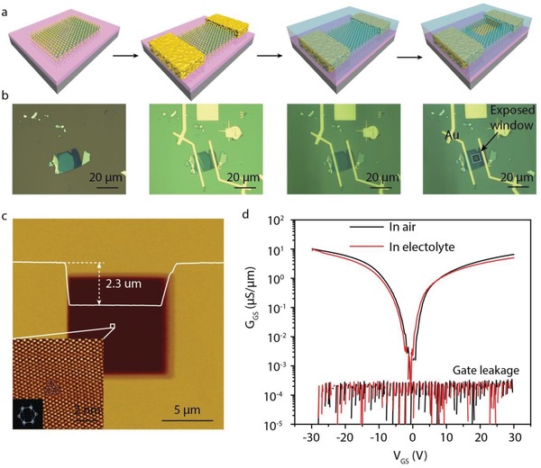
Figure 1.

The device fabrication on WSe2 basal plane. a) A schematic diagram of the fabrication process and b) a realistic optical image of WSe2 device. c) The AFM height image of the protected PMMA layer, where the window is exposed by EBL only on the WSe2 basal plane. The inset shows the low pass filtered atomic pattern acquired from the center region by lateral force microscopy. d) The electrical performance of WSe2 device in the air and an electrolyte. The electrolyte is 0.5 mol L−1 H2SO4 solution.
