
Figure 2.
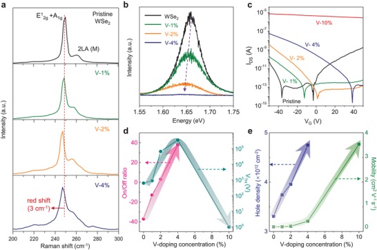
p‐Doping effect of V‐substitution to WSe2. a,b) Raman (a) and PL (b) spectra of V‐doped WSe2 monolayer at an excitation wavelength of 532 nm in terms of V‐doping concentration. c) I DS–V G curves of V‐doped WSe2 transistors under V DS = 0.5 V. d,e) On/off ratio (I −50 V/I off) and threshold voltage (d) field‐effect hole mobility and intrinsic hole carrier concentration (e) as a function of V‐doping concentration.