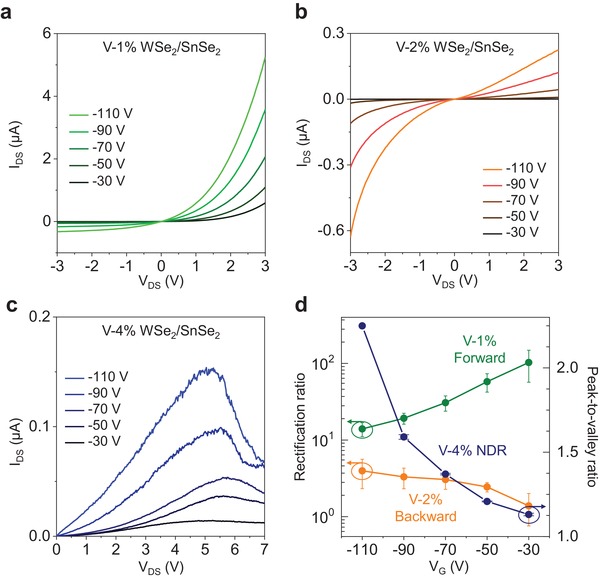
Figure 4.

Gate‐tunable behaviors of V‐doped WSe2/SnSe2 devices. a–c) I DS–V DS output curves of the forward rectifying diode, backward rectifying diode, and NDR tunneling under various gate biases. d) Device rectification ratio (I 3V/I −3 V in the forward direction, and I −3 V/I 3V in the backward direction) and NDR peak‐to‐valley ratio as a function of gate bias with reasonable error bars, demonstrating the reproducibility.
