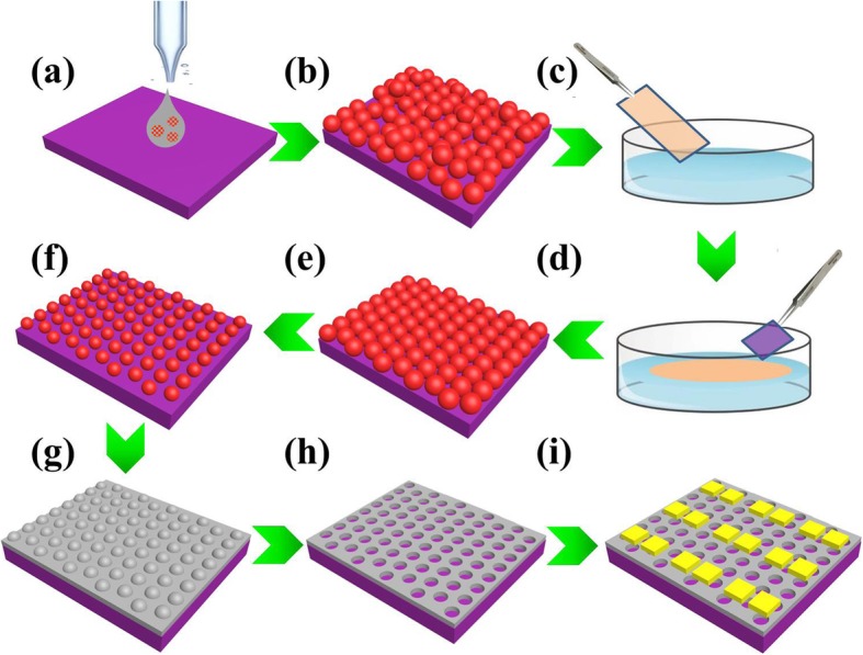
Fig. 1.

Schematic illustration of the fabrication processes for cross-linked network based gas sensors. a Drop PS microspheres solution onto a 2 cm × 4 cm Si3N4 substrate. b PS microspheres self-assemble into an irregular monolayer. c Insert the above Si3N4 substrate into deionized water. d PS microspheres reassemble into a close-packed regular array floating at the air/water surface. e Another 1 cm × 1 cm Si3N4 substrate was used to carefully pick up the two-dimensional array. f Plasma etching was executed to control the size of PS microspheres. g Deposit the SnO2/NiO thin film by sputtering technique. h Remove the PS microspheres to form a cross-linked SnO2/NiO network. i Deposit the gold electrodes array
