

Abstract

Novel schemes based on the design of complex three-dimensional (3D) nanoscale architectures are required for the development of the next generation of advanced electronic components. He+ focused-ion-beam (FIB) microscopy in combination with a precursor gas allows one to fabricate 3D nanostructures with an extreme resolution and a considerably higher aspect ratio than FIB-based methods, such as Ga+ FIB-induced deposition, or other additive manufacturing technologies. In this work, we report the fabrication of 3D tungsten carbide nanohelices with on-demand geometries via controlling key deposition parameters. Our results show the smallest and highest-densely packed nanohelix ever fabricated so far, with dimensions of 100 nm in diameter and aspect ratio up to 65. These nanohelices become superconducting at 7 K and show a large critical magnetic field and critical current density. In addition, given its helical 3D geometry, fingerprints of vortex and phase-slip patterns are experimentally identified and supported by numerical simulations based on the time-dependent Ginzburg–Landau equation. These results can be understood by the helical geometry that induces specific superconducting properties and paves the way for future electronic components, such as sensors, energy storage elements, and nanoantennas, based on 3D compact nanosuperconductors.
Keywords: Helium ion microscope, three-dimensional nanoprinting, focused-ion-beam-induced deposition, nanosuperconductors, phase slips, Ginzburg−Landau equation
Superconductors are integrated in major equipment and machinery, for instance as part of powerful magnets,1 employed for nuclear magnetic resonance,2 fusion reactors,3 and particle accelerators.4 Moreover, they have become excellent materials for energy storage,5 electrical generators,6 magnetic sensors,7 and high-frequency filters and switches.8,9 These superconductors normally need nanoengineering to achieve the required performance in those applications.10 Besides, nanostructured superconductors are central elements in refined quantum computing architectures such as one-dimensional (1D) nanowire-based quantum oscillators11 and highly integrated Josephson junction networks.12 From a basic research point of view, superconducting nanostructures are fascinating objects to study vortex confinement caused by defects, geometry and/or topology to preserve the dissipation-free energy state.13,14
Innovative schemes have taken advantage of the third dimension for the development of high-performance and energy-efficient electronic components.15 Thus, three-dimensional (3D) nanosuperconductivity could represent a breakthrough for future electronics components, particularly for sensors, energy-storage components, and quantum computing. A significant improvement of the microwave radiation detection has been demonstrated through the fabrication of a superconducting bolometer by folding two-dimensional (2D) superconductor structures into 3D helical belts.16 However, until now, few works of real 3D superconducting nanostructures have been reported,17−21 mainly because their fabrication and characterization are still challenging.
In the last decades, Ga+ focused-ion-beam-induced deposition (FIBID) has been used to grow functional 3D materials.22−27 Particularly, 3D superconducting W-based nanowires, with superconducting critical temperature Tc ∼ 5 K and upper critical magnetic field μ0Hc2(0) ∼ 9.5 T,17−19 and NbC nanowires with Tc ≈ 11 K,21 were recently grown using, respectively, W(CO)6 and Nb(NMe2)3(N-t-Bu) precursor materials. Nevertheless, the resolution in this process is mainly limited by the Ga+ beam diameter (∼5 nm) and its high lateral scattering. This prevents the growth of sub-100 nm 3D nanostructures.
A recent generation of focused particle beam for 3D nanoprototyping is the helium ion microscope (HIM),28 based on He+ gas-FIB source with a probe size as small as ≈0.3 nm. Thus, HIM represents an enormous step forward for 3D nanoprinting due to the small beam diameter and low proximity effect,29 creating vertical pillars of PtC and tungsten carbide (WC) with diameters down to 40 nm.30,31 In a recent study, some of the authors have reported on the fabrication of 3D superconducting hollow nanowires as small as 32 nm in diameter, with a Tc ≈ 6.4 K and high critical magnetic field and current density,20 opening a new path for the fabrication of more complex 3D nano-objects that could be implemented as future components in electronics.
In this work, we present the fabrication of 3D WC superconducting nanohelices on demand by using a HIM. The nanohelices geometry is successfully controlled with pitches (LT) between 200 nm and 2.3 μm, nanohelix diameters (DNH) from 100 to 295 nm, and nanowire diameter (DNW) as small as 45 nm. These 3D nanohelices display superconductivity below 7 K (Tc) as well as high upper critical magnetic fields μ0Hc2 ≈ 15 T and high critical current densities Jc ≈ 0.2 MA/cm2. The magnetotransport properties at low temperature and under magnetic fields show characteristic features of vortex and phase slip patterns associated with the nanohelix topology and 3D geometry. These experimental data are in good agreement with numerical simulations based on the time-dependent Ginzburg–Landau equation.
We use a HIM focused to ∼1 nm in combination with a W(CO)6 precursor to grow individual and vertical 3D WC nanohelices. The precursor flux is delivered into the process chamber and adsorbs to the substrate’s surface, whereas the He+ FIB spot describes a circular shape with a proper overlapping between two consecutive spots and a beam dwell time that favors continuous growth along the third dimension. By keeping the optimized beam parameters, a nanohelix is fabricated, increasing the number of turns of the circular shape pattern, as depicted in the sketch and in the SEM image of a representative nanohelix (deposition parameters: Ibeam ≈ 1 pA, beam spacing = 10 nm, nominal diameter = 75 nm, beam dwell time = 700 ms, turns = 23) shown in Figure 1.
Figure 1.

(Left) Sketch of the growth of 3D nanohelix by He+-FIBID. (Right) SEM image of a WC 3D nanohelix of type 1, in which pattern parameters are indicated, DNW = nanowire diameter, DNH = nanohelix diameter (100 nm in this specific case), LT = turn length or pitch, and LNH = nanohelix length (52° tilted stage). The specific deposition parameters for the helix shown are Ibeam ≈ 1 pA, beam spacing = 10 nm, nominal diameter = 75 nm, beam dwell time = 700 ms, and turns = 23.
To find the optimal parameters for the fabrication of 3D nanohelices, we investigate the resolution limits and dimensional control by varying the diameter and beam dwell time. A linear dependence of the pitch as a function of the beam dwell time for nominal diameters ranging from 75 to 200 nm has been found (see Figure S1, Table S1, and Figure S2). The use of such method enables us to fabricate 3D helical nanostructures on demand, as shown in Figure 2. The specific deposition parameters and real dimensions of nanohelices of types 1–8 are listed in Table 1. Particularly, nanohelices of types 1–5 were grown by keeping fixed the nominal circular diameter to 75 nm and varying the beam dwell time from 700 to 2400 ms. Using these parameters, the achieved nanohelix diameter ranges from 100 to 146 nm and the pitch from 200 nm to 1 μm. Nanohelix of type 1 is the smallest and highest-densely packed nanohelix ever fabricated so far, with 100 nm in diameter, 200 nm of pitch, and 23 turns. Nanohelices of types 6–8 were grown by keeping fixed the nominal circular diameter to 200 nm and varying the beam dwell time from 650 to 2000 ms. By using these parameters, the nanohelix diameters range from 277 to 295 nm and pitches from 430 nm to 2.3 μm. Further highlights of the fabrication procedure include the very small nanowire diameter of 45 nm and the short process time of only a few minutes. More details regarding growth conditions are described in the Supporting Information (methods section).
Figure 2.

SEM images of WC nanohelices of several types (from 1–8) grown by He+-FIBID (52° tilted stage). ΔV represents the locations of the voltage contacts. Inset in the SEM image type 1 shows the top view of the nanohelix (measured bar = 100 nm).
Table 1. Growth Parameters and Nominal and Real Dimensions of WC Nanohelices Shown in Figure 1a.
| nanohelix no. | 1 | 2 | 3 | 4 | 5 | 6 | 7 | 8 |
|---|---|---|---|---|---|---|---|---|
| ion current | 0.96 | 0.92 | 0.92 | 0.86 | 1.47 | 1.23 | 1.32 | 1.31 |
| nominal nanohelix diameter (nm) | 75 | 75 | 75 | 75 | 75 | 200 | 200 | 200 |
| repeats | 23 | 16 | 12 | 8 | 6 | 15 | 8 | 4 |
| dwell time (ms) | 700 | 1000 | 1400 | 1800 | 2400 | 650 | 950 | 2000 |
| real nanohelix diameter, DNH (nm) | 100 | 115 | 116 | 108 | 146 | 277 | 295 | 277 |
| nanowire diameter, DNW (nm) | 50 | 58 | 50 | 51 | 58 | 58 | 58 | 45 |
| pitch, LT (nm) | 200 | 220 | 440 | 550 | 1000 | 430 | 925 | 2300 |
| curvature (nm–1 × 10⁻³) | 14.2 | 12.7 | 7 | 5.1 | 2.4 | 5.8 | 3.4 | 0.9 |
| torsion (nm–1 × 10⁻³) | 9.1 | 7.7 | 8.5 | 8.3 | 5.2 | 2.9 | 3.4 | 2.4 |
For a helix parametrized through
the radius R and pitch (2πb), x(t) = R sin t, y(t) = R cos t, z(t) = bt, the curvature k1 and torsion k2 provide an equivalent representation:43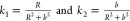 . We have selected the “radius–pitch”
representation since these parameters directly correlate with the
crucial physical parameters of the same dimensionality: coherence
length and penetration depth.
. We have selected the “radius–pitch”
representation since these parameters directly correlate with the
crucial physical parameters of the same dimensionality: coherence
length and penetration depth.
For magnetotransport measurements, the 3D nanohelices were placed flat on the SiO2 layer of a Si/SiO2 substrate by means of a nanomanipulator. This step is challenging due to the elastic behavior of the nanohelices (see Movie S1 in the Supporting Information for details). Then, four Pt FIBID contacts were grown to connect the nanohelices to prepatterned Ti pads. Finally, four-probe electrical measurements at low temperature (from 300 to 0.5 K) and under perpendicularly applied magnetic field to the substrate plane (from 0 to 9 T) were performed (see Figure S3 and Supporting Information for details of deposition parameters). This process was performed for nanohelices of types 1, 4, 6, and 7 (see Figure 2 and Table 1). On the one hand, we have studied small, both densely packed and sparsely packed nanohelices, that is, nanohelices of types 1 and 4 with DNH ∼ 100 nm and DNW ∼ 50 nm, with a pitch of 200 nm for type 1 and 550 nm for type 4. On the other hand, large and both densely packed and sparsely packed nanohelices were also investigated. These are nanohelices of types 6 and 7 with DNH ∼ 280 nm and DNW ∼ 58 nm, with a pitch of 430 nm for type 6 and 925 nm for type 7.
Nanohelices show resistance drops from the normal to the superconducting
state at Tc (0.5 RN) values between 6.23 and 7.06 K (see Figure 3a and Table 2). Figure 3b shows their upper critical magnetic field μ0Hc2 (0.9 RN) as a function of temperature. μ0Hc2 is extracted from the resistance versus temperature
curves under perpendicular magnetic field (i.e., inset of Figure 3b). We fit μ0Hc2(T) to a simple
power law equation μ0Hc2(T) ∝ (1 – T/Tc)n. For a 2D film
and a perpendicular magnetic field or a 3D bulk sample, we expect
usual Werthammer–Helfand–Hohenberg behavior,32 with n ∼ 1. For a 1D
wire, we expect n = 0.5.14 Here we find n in between, ranging from 0.72 to
0.78 for nanohelices with a nanowire diameter of 50 and 58 nm, respectively.
The deviation from the usual 1D and 3D behaviors suggests that nanohelices
have an intermediate superconducting behavior.33 Moreover, we find that μ0Hc2(0 K) ranges from 12.1 to 15.3 T in different helices.
Using the orbital limit estimation of μ0Hc2(T) = Φ0/2πξ2(T), the Cooper
pair coherence length, ξ, at 0 K is found to range from 4.64
to 5.22 nm. Considering nanohelices as type II superconductors in
the weak coupling regime and in the dirty limit, the magnetic field
penetration length (λ) can be estimated applying the following
expression  derived from the Gor’kov theory.34 The λ values range from 603 to 733 nm.
Figure 3.

(a) Normalized resistance for nanohelices of types indicated in the legend as a function of temperature at 0 T. RN is the resistance at the normal state, at T = 10 K. Inset shows resistance versus temperature for nanohelix of type 7. Ibias = 100 nA. (b) Upper critical magnetic field (μ0Hc2) as a function of temperature for nanohelices of types indicated in the legend. Data are fitted to a power low equation. Inset shows resistance as a function of temperature for nanohelix of type 7 under perpendicular magnetic field, from 0 to 9 T.
Table 2. Superconducting Parameters of Nanohelices of Types 1, 4, 6, and 7 Estimated from Experimental Magnetotransport Measurements.
| nanohelix no. | 1 | 4 | 6 | 7 |
|---|---|---|---|---|
| RN (Ω) | 1281 | 1936 | 1796 | 3672 |
| no. of turns | 4 | 3 | 2 | 3 |
| Tc (K) | 6.73 | 6.50 | 6.23 | 7.06 |
| μ0Hc2 (0 K) (T) | 14.3 | 12.1 | 12.8 | 15.3 |
| n | 0.72 ± 0.01 | 0.72 ± 0.04 | 0.76 ± 0.02 | 0.78 ± 0.02 |
| ξ0 (nm) | 4.80 | 5.22 | 5.07 | 4.64 |
| λ (nm) | 603 | 629 | 733 | 695 |
| Jc (0.5 K, 0 T) (MA/cm2) | 0.23 | 0.17 | 0.09 | 0.11 |
| Jd (0.5 K, 0 T) (MA/cm2) | 17.8 | 15.3 | 10.8 | 14.1 |
The highest value of Jc (0.5 K, 0 T) ∼ 0.23 MA/cm2 is found for the smallest and more-densely packed nanohelix (type 1), which is twice higher than the value for sparsely packed nanohelices (types 6 and 7) (see Figure S4 in the Supporting Information). Jc values are around 80 times lower than the depairing current density,35 Jd (0.5 K, 0 T) ∼ 17.8 MA/cm2 (see Table 2), at which the electromagnetic energy due to the current flow is equal to the superconducting condensation energy. Such a difference is found almost invariably in all superconductors indicating that dissipation sets in well below the depairing energy due to formation of phase slips or vortices significantly below the depairing current. Besides, sample inhomogeneities, such as grain boundaries, differences in composition, nanodefects or amorphization over these small dimensions can produce a depression effect on the critical current density of the nanohelices. To conclude, the calculated superconducting parameters of 3D nanohelices are comparable with those found in He+ FIBID out-of-plane hollow nanowires,20 and He+ FIBID in-plane nanowires used in hybrid microwave resonators.36 The kinetic inductance for this material is ∼15 pH/, which is 250 times higher than the geometrical inductance,36 making them good candidates for the fabrication of highly packed 3D nanoresonators.
We have observed an enhancement of the dissipation-free ground state, μ0Hmin (defined as the field value at which resistance reach 0.1RN) for the nanohelix type 7 (Figure 4(a)). It is 35% larger compared to hollow nanowires grown by He+ FIBID.20 This suggests that the helix provides much stronger pinning as compared to straight nanowires.37 We will develop this in detail below, but we point out that such an improvement can be used to build better superconducting logic gates,38 quantum switches39 and single-photon detectors.40−42
Figure 4.

(a) Critical magnetic fields as a function of temperature for nanohelix of type 7. μ0Hc2 is estimated from 0.9RN and μ0Hmin from 0.1RN. These values are extracted from R vs T curves (under perpendicular magnetic field, from 0 to 9 T, black symbols) and from R vs μ0H curves (under perpendicular magnetic field, from 0 to 20 T, gray symbols), Ibias= 0.1 μA. Data is fitted to a power law dependence. (b) Tilt-angle applied magnetic field dependence on μ0Hc2 for nanohelix of type 7. μ0Hc2 values are extracted from R vs μ0H curves, Ibias= 0.1 μA.
On the other hand, the dependence of μ0Hc2 for the nanohelix when tilting the magnetic field is not strong, but appreciable (Figure 4(b)). This suggests that the direction of the magnetic field, compared to the precise geometry, plays a significant role in the upper critical field (we discuss this in more detail in the Supporting Information).
An interesting feature only visible in resistance-versus-current measurements for the nanohelix type 6 is that the resistive transition occurs in various steps, as observed in measurements under fixed perpendicular magnetic field of 1 and 2 T (see Figure 5). Nanohelices of types 1, 4, and 7 do not show this feature (see Figure S5). In order to provide some insight into this behavior, numerical simulations based on the time-dependent Ginzburg–Landau equation coupled with Poisson equation have been performed by finite-difference time-domain method (see Supporting Information, numerical simulations). This analysis reveals several patterns of the order parameter corresponding to the spatial distribution of the normal to the surface component of the magnetic field over the surface of the helical nanostructure. These patterns are represented in the right panels of Figure 5(a) and (b) for magnetic fields 1 and 2 T, respectively. The order parameter distribution over the surface of the helical structure is shown at different values of the applied transport current (in units of the critical current). The voltage generated by an individual vortex in motion for all patterns leads to a finite resistance of the order of 1 Ω. Experimentally observed jumps (higher than 100 Ω) in the Resistance vs Current charactertistics are about 2 orders of magnitude higher than the resistance induced by an individual vortex, which follows from our numerical simulation (see Supporting Information). The most probable reason for the observed jumps is therefore the occurrence of phase slips, which start to appear at transport current values shown in Figure 5. The transition of two half-turns into the full phase-slip regime causes the resistance to increase by about 1000 Ω, whereas the presence of the phase slip in all half-turns without the vortex dynamics results in a resistance of about 2250 Ω. The simulated order parameter at a magnetic field B = 1 T shown in Figure 5(a) does not seem to reveal vortices in static or dynamic states. From an arbitrary initial state (for which a random distribution was taken), the order parameter evolves to one of the three following quasi-stationary patterns: (i) pure vortex state (the amount of vortices is in the range from 0 to N), (ii) mixed one–vortices plus order parameter depression regions (phase slip), and (iii) pure order parameter depression regimes. We suggest that the whole half turn, at which the order parameter depression appears, switches to the normal state due to the Joule heating as shown in Figures S6. In regions where the absolute value of the normal to surface magnetic field is minimal, the order parameter depression extent is suppressed. This mechanism explains the experimental step-like resistance vs current dependence. Our numerical simulations are described in the Supporting Information (numerical simulations section, inputs from Tables S2 and S3. As distinct from the planar 2D superconductor structures, the complex 3D geometry of nanohelices determines topologically nontrivial screening currents and confinement potentials that cardinally depend on radius and pitch (or, equivalently, curvature and torsion) and imply, as shown below, occurrence of different patterns of topological defects. For all structures, we have observed similar behavior when the applied current increases from 0 to the critical value: the modulus of the order parameter evolves from a homogeneous state, which describes the pure superconducting phase, to different patterns of vortices, then to different phase-slip patterns, finally resulting in the normal state. We have found that a phase-slip pattern itself may depend on the number of turns. In order to check how phase-slip patterns evolve with increasing number of turns, we have performed a simulation for structures with fixed width (50 nm), helical diameter (100 nm), and pitch (200 nm) under a magnetic field of 2 T. These geometrical characteristics of the simulated structures correspond to the experimental helix of type 1. Results of this simulation for fixed applied transport current (I ∼ 0.6Ic) are shown in Figure S7. For the structure with one turn, phase slips are represented by three extended regions over the half-turns. Phase slips occupy approximately 80% of the area of the structure. For the structure with two turns, there are 5 regions with phase slips, while the relative size of each phase slip region being smaller than the relative size of a phase-slip region for the structure with one turn. The trend of decreasing the size of the phase-slip regions and increasing their number continues for the structure with three turns. For the structure with four turns, the phase-slip regions disappear in some parts of the structure. The increment of the resistance is proportional to the overall size of the phase-slip regions, so, when the phase-slip pattern is represented by a number of small regions, each new region gives a small increment to the resistance (the case realized in helices of types 1, 4, 7). In this case, there will occur no shelf-like features in the Resistance-vs-Current dependence within the experimental conditions. Figures S7, S8 and S9 demonstrate how chirality of the nanohelices determines the order-parameter patterns that are quite distinct from those in the planar structures and thus provide an insight into the occurrence of the shelf-like features in the Resistance-vs-Current characteristics in some nanohelices, while there are no such features in other nanohelices.
Figure 5.

Experimental Resistance-vs-Current characteristics (left panels) for the nanohelix of type 6, and simulated order parameter distributions plotted over the 2D surface of the helical structure (right panels) for the magnetic fields 1 T (upper–right panel) and 2 T (lower–right panel). The values of the applied transport current in units of the critical current are indicated in the panels. The critical currents are evaluated from the experimental data to be 3.3 μA for 1 T and 3.0 μA for 2 T. Different vortex and phase-slip patterns correspond to steps of resistance (the correspondence is shown by the arrows).
Despite the overall superconducting properties (Tc, Hc2, Jc) of all nanohelices are similar given the same composition, their behavior is different in various cases, because the complex 3D geometry of a nanohelix leads to disconnected screening currents and richly diversified confinement potentials that shape drastically different patterns of vortices (see, e.g., different multiple disconnected vortex arrays in nanohelices with different numbers of windings)37 and phase slips (see Figure S7).
To conclude, we report a direct-write methodology to fabricate 3D superconducting nanohelices on demand by using W(CO)6 precursor with a highly focused He+ beam. The resulting 3D nanohelices have diameters as small as 100 nm and pitches down to 200 nm, making them the smallest and highest-densely packed nanohelices ever grown, which is unachievable with other manufacturing techniques. By studying their magnetotransport properties, we have found that they exhibit superconducting properties below Tc= 7 K as well as high critical magnetic field and critical current density. Moreover, signatures of vortex and phase-slip patterns due to their helical 3D geometries are experimentally found. This behavior is attributed to the specific order parameter and magnetic field distributions, which favor the formation of superconducting vortices and order parameter depressions (phase slips) in given regions, as supported by our numerical simulations. Our methodology represents an accurate and reproducible bottom-up approach for the fabrication of innovative, better performing, and more compact 3D nanoarchitectures (Figure S12).
Acknowledgments
This work was supported by the financial support from Spanish Ministry of Economy and Competitiveness through the projects MAT2017-82970-C2-2-R, PIE201760E027, including FEDER funding, FIS2017-84330-R, MDM-2014-0377, EU ERC (grant agreement no. 679080), COST grant no. CA16128, and STSM grant 41199 for V.M.F. from COST Action CA16218, from the EU-H2020 research and innovation programme under grant agreement no. 654360 NFFA-Europe, from regional Gobierno de Aragón (grants E13_17R) with European Social Fund (Construyendo Europa desde Aragón) and Comunidad de Madrid through project Nanofrontmag-CM (grant no. S2013/MIT-2850). Authors acknowledge the LMA-INA for offering access to their instruments and expertise and the use of Servicio General de Apoyo a la Investigación-SAI, Universidad de Zaragoza, particularly the Servicio de Medidas Físicas. The support of the German Research Foundation (DFG) via grant FO 956/5-1 is gratefully acknowledged. Authors acknowledge the Center for Information Services and High Performance Computing (ZIH) at TU Dresden for offering access to the HPC system. This work was supported by HFML-RU/NWO-I, member of the European Magnetic Field Laboratory (EMFL). It is part of the research program no. 132 “High Field Magnet Laboratory: a global player in science in high magnetic fields” financed by The Netherlands Organisation for Scientific Research (NWO).
Supporting Information Available
The Supporting Information is available free of charge at https://pubs.acs.org/doi/10.1021/acs.nanolett.9b03153.
Author Contributions
R.C. and J.M.D.T. led the project and conceived the experiments. R.C. and D.M. grew the WC 3D nanohelices by using a He+ microscope. R.C. made the auxiliary contacts to the nanohelices, measured their electrical transport behavior, performed the subsequent data analysis, and wrote the first version of the manuscript. O.G.S. and V.M.F. developed key conceptual ingredients for the interpretation. R.O.R. and E.I.S. performed numerical simulations. U. Z. and R. C. performed electrical transport experiments of nanohelices in tilted magnetic fields at the High Magnetic Field Laboratory in Nijmegen. I.G. and H.S. collaborated in the sample design and in the discussion of the results. All authors discussed the results, the manuscript, contributed to it, and have given approval to the final version of the manuscript.
The authors declare no competing financial interest.
Supplementary Material
References
- Larbalestier D. C.; Jiang J.; Trociewitz U. P.; Kametani F.; Scheuerlein C.; Dalban-Canassy M.; Matras M.; Chen P.; Craig N. C.; Lee P. J.; Hellstrom E. E. Nat. Mater. 2014, 13 (4), 375–381. 10.1038/nmat3887. [DOI] [PubMed] [Google Scholar]
- Reif F. Phys. Rev. 1956, 102 (5), 1417–1418. 10.1103/PhysRev.102.1417. [DOI] [Google Scholar]
- Bromberg L.; Tekula M.; El-Guebaly L.; Miller R. Fusion Eng. Des. 2001, 54 (2), 167–180. 10.1016/S0920-3796(00)00432-4. [DOI] [Google Scholar]
- Schmuser P. Rep. Prog. Phys. 1991, 54 (5), 683–730. 10.1088/0034-4885/54/5/001. [DOI] [Google Scholar]
- Larbalestier D.; Gurevich A.; Feldmann D. M.; Polyanskii A. Nature 2001, 414 (6861), 368–377. 10.1038/35104654. [DOI] [PubMed] [Google Scholar]
- Barnes P. N.; Sumption M. D.; Rhoads G. L. Cryogenics 2005, 45 (10–11), 670–686. 10.1016/j.cryogenics.2005.09.001. [DOI] [Google Scholar]
- Tesche C. D.; Clarke J. J. Low Temp. Phys. 1977, 29 (3–4), 301–331. 10.1007/BF00655097. [DOI] [Google Scholar]
- Martinez J.; Hijazi Y.; Brzhezinskaya M.; Bogozi A.; Noel J.; Vlasov Y. A.; Larkins G. L. Phys. C 2007, 466 (1–2), 101–105. 10.1016/j.physc.2007.06.006. [DOI] [Google Scholar]
- Noel J.; Hijazi Y.; Martinez J.; Vlasov Y. A.; LarkinsJr G. L. Supercond. Sci. Technol. 2003, 16 (12), 1438–1441. 10.1088/0953-2048/16/12/026. [DOI] [Google Scholar]
- Gutiérrez J.; Llordés A.; Gázquez J.; Gibert M.; Romà N.; Ricart S.; Pomar A.; Sandiumenge F.; Mestres N.; Puig T.; Obradors X. Nat. Mater. 2007, 6 (5), 367–373. 10.1038/nmat1893. [DOI] [PubMed] [Google Scholar]
- Giordano N. Phys. Rev. Lett. 1988, 61 (18), 2137–2140. 10.1103/PhysRevLett.61.2137. [DOI] [PubMed] [Google Scholar]
- Fazio R. Phys. Rep. 2001, 355 (4), 235–334. 10.1016/S0370-1573(01)00022-9. [DOI] [Google Scholar]
- Tonomura A.; Kasai H.; Kamimura O.; Matsuda T.; Harada K.; Nakayama Y.; Shimoyama J.; Kishio K.; Hanaguri T.; Kitazawa K.; Sasase M.; Okayasu S. Nature 2001, 412 (6847), 620–622. 10.1038/35088021. [DOI] [PubMed] [Google Scholar]
- Córdoba R.; Baturina T. I.; Sesé J.; Yu Mironov A.; De Teresa J. M.; Ibarra M. R.; Nasimov D. A.; Gutakovskii A. K.; Latyshev A. V.; Guillamón I.; Suderow H.; Vieira S.; Baklanov M. R.; Palacios J. J.; Vinokur V. M. Nat. Commun. 2013, 4 (1), 1437. 10.1038/ncomms2437. [DOI] [PubMed] [Google Scholar]
- Shulaker M. M.; Hills G.; Park R. S.; Howe R. T.; Saraswat K.; Wong H.-S. P.; Mitra S. Nature 2017, 547 (7661), 74–78. 10.1038/nature22994. [DOI] [PubMed] [Google Scholar]
- Lösch S.; Alfonsov A.; Dobrovolskiy O. V.; Keil R.; Engemaier V.; Baunack S.; Li G.; Schmidt O. G.; Bürger D. ACS Nano 2019, 13 (3), 2948–2955. 10.1021/acsnano.8b07280. [DOI] [PubMed] [Google Scholar]
- Li W.; Gu C.; Warburton P. A. J. Nanosci. Nanotechnol. 2010, 10 (11), 7436–7438. 10.1166/jnn.2010.2850. [DOI] [PubMed] [Google Scholar]
- Romans E. J.; Osley E. J.; Young L.; Warburton P. A.; Li W. Appl. Phys. Lett. 2010, 97 (22), 222506. 10.1063/1.3521262. [DOI] [Google Scholar]
- Li W.; Fenton J. C.; Cui A.; Wang H.; Wang Y.; Gu C.; McComb D. W.; Warburton P. A. Nanotechnology 2012, 23 (10), 105301. 10.1088/0957-4484/23/10/105301. [DOI] [PubMed] [Google Scholar]
- Córdoba R.; Ibarra A.; Mailly D.; De Teresa J. M. Nano Lett. 2018, 18 (2), 1379–1386. 10.1021/acs.nanolett.7b05103. [DOI] [PubMed] [Google Scholar]
- Porrati F.; Barth S.; Sachser R.; Dobrovolskiy O. V.; Seybert A.; Frangakis A. S.; Huth M. ACS Nano 2019, 13, 6287. 10.1021/acsnano.9b00059. [DOI] [PubMed] [Google Scholar]
- Matsui S.; Kaito T.; Fujita J.; Komuro M.; Kanda K.; Haruyama Y. In Papers from the 44th international conference on electron, ion, and photon beam technology and nanofabrication; AVS: Rancho Mirage, CA, 2000; Vol. 18, pp 3181–3184. [Google Scholar]
- Morita T.; Kometani R.; Watanabe K.; Kanda K.; Haruyama Y.; Hoshino T.; Kondo K.; Kaito T.; Ichihashi T.; Fujita J.; Ishida M.; Ochiai Y.; Tajima T.; Matsui S. J. Vac. Sci. Technol., B: Microelectron. Process. Phenom. 2003, 21 (6), 2737. 10.1116/1.1630329. [DOI] [Google Scholar]
- Esposito M.; Tasco V.; Todisco F.; Benedetti A.; Sanvitto D.; Passaseo A. Adv. Opt. Mater. 2014, 2 (2), 154–161. 10.1002/adom.201300323. [DOI] [Google Scholar]
- Esposito M.; Tasco V.; Cuscunà M.; Todisco F.; Benedetti A.; Tarantini I.; Giorgi M. De; Sanvitto D.; Passaseo A. ACS Photonics 2015, 2 (1), 105–114. 10.1021/ph500318p. [DOI] [Google Scholar]
- Fujii T.; Iwasaki K.; Munekane M.; Takeuchi T.; Hasuda M.; Asahata T.; Kiyohara M.; Kogure T.; Kijima Y.; Kaito T. J. J. Micromech. Microeng. 2005, 15 (10), S286–S291. 10.1088/0960-1317/15/10/S06. [DOI] [Google Scholar]
- Nakai Y.; Kang Y.; Okada M.; Haruyama Y.; Kanda K.; Ichihashi T.; Matsui S. Jpn. J. Appl. Phys. 2010, 49 (6), 06GH07. 10.1143/JJAP.49.06GH07. [DOI] [Google Scholar]
- Scipioni L.; Stern L. A.; Notte J.; Sijbrandij S.; Griffin B. Adv. Mater. Process. 2008, 166 (6), 27. [Google Scholar]
- Maas D.; van Veldhoven E.; Chen P.; Sidorkin V.; Salemink H.; van der Drift E.; Alkemade P.. Nanofabrication with a helium ion microscope. In Metrology, Inspection, and Process Control for Microlithography XXIV; Raymond C. J., Ed.; SPIE Press: Bellingham, WA, 2010; Vol. 7638, p 763814. [Google Scholar]
- Alkemade P. F. A.; Miro H. Appl. Phys. A: Mater. Sci. Process. 2014, 117 (4), 1727–1747. 10.1007/s00339-014-8763-y. [DOI] [Google Scholar]
- Kohama K.; Iijima T.; Hayashida M.; Ogawa S. J. Vac. Sci. Technol., B: Nanotechnol. Microelectron.: Mater., Process., Meas., Phenom. 2013, 31 (3), 031802. 10.1116/1.4800983. [DOI] [Google Scholar]
- Guillamón I.; Suderow H.; Fernández-Pacheco A.; Sesé J.; Córdoba R.; De Teresa J. M.; Ibarra M. R.; Vieira S. Nat. Phys. 2009, 5 (9), 651. 10.1038/nphys1368. [DOI] [Google Scholar]
- Makise K.; Terai H.; Tominari Y.; Tanaka S.; Shinozaki B. Sci. Rep. 2016, 6 (1), 27001. 10.1038/srep27001. [DOI] [PMC free article] [PubMed] [Google Scholar]
- Gor’kov L. P. J. Exptl. Theor. Phys. 1959, 36 (36), 1918–1923. [Google Scholar]
- Dinner R. B.; Robinson A. P.; Wimbush S. C.; MacManus-Driscoll J. L.; Blamire M. G. Supercond. Sci. Technol. 2011, 24 (5), 055017. 10.1088/0953-2048/24/5/055017. [DOI] [Google Scholar]
- Basset J.; Watfa D.; Aiello G.; Féchant M.; Morvan A.; Estève J.; Gabelli J.; Aprili M.; Weil R.; Kasumov A.; Bouchiat H.; Deblock R. Appl. Phys. Lett. 2019, 114 (10), 102601. 10.1063/1.5080925. [DOI] [Google Scholar]
- Fomin V. M.; Rezaev R. O.; Levchenko E. A.; Grimm D.; Schmidt O. G. J. Phys.: Condens. Matter 2017, 29 (39), 395301. 10.1088/1361-648X/aa7dbe. [DOI] [PubMed] [Google Scholar]
- Puig T.; Rosseel E.; Baert M.; Van Bael M. J.; Moshchalkov V. V.; Bruynseraede Y. Appl. Phys. Lett. 1997, 70 (23), 3155–3157. 10.1063/1.119118. [DOI] [Google Scholar]
- Chiorescu I.; Nakamura Y.; Harmans C. J. P. M.; Mooij J. E. Science 2003, 299 (5614), 1869–1871. 10.1126/science.1081045. [DOI] [PubMed] [Google Scholar]
- Kadin A. M.; Leung M.; Smith A. D. Phys. Rev. Lett. 1990, 65 (25), 3193–3196. 10.1103/PhysRevLett.65.3193. [DOI] [PubMed] [Google Scholar]
- Dauler E. A.; Kerman A. J.; Rosenberg D.; Pan S.; Grein M. E.; Molnar R. J.; Correa R. E.; Bawendi M. G.; Berggren K. K.; Moores J. D.; Boroson D. M. Proceedings from the IEEE Photonic Society 24th Annual Meeting, Arlington, VA, October, 2011; IEEE: Piscataway, NJ, 2011; pp 350–351.
- Natarajan C. M.; Tanner M. G.; Hadfield R. H. Supercond. Sci. Technol. 2012, 25 (6), 063001. 10.1088/0953-2048/25/6/063001. [DOI] [Google Scholar]
- Dubrovin B. A.; Fomenko A. T.; Novikov S. P.. Modern Geometry -- Methods and Applications : Part I. The Geometry of Surfaces, Transformation Groups, and Fields; Springer: New York, 1984. [Google Scholar]
Associated Data
This section collects any data citations, data availability statements, or supplementary materials included in this article.