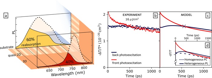
Figure 4.
(a) PL spectra (dashed line, corrected for self-absorption) of the quasi-2D and 3D lead iodide perovskite regions of the thin film. The highlighted area indicates the spectral overlap with the absorption spectrum. The calculated photon recapture probabilities are 40% for 3D emission and 60% for quasi-2D emission. (b) OPTP dynamics measured with illumination incident on the front (red) or back (dark blue) side of the thin film, with fluence 16 μJ/cm2. Dots represent experimental data and solid lines in (c) are simulated transients (accounting for charge diffusion and photon reabsorption under the assumption of heterogeneous PL emission; recombination rate constants were obtained from the fits to experimental data). (d) Simulated OPTP photoconductivity dynamics for photoexcitation incident on the front (red) or back (dark blue) of the thin film, both accounting for charge diffusion and photon reabsorption, but considering either homogeneous (dotted lines) or heterogeneous (solid lines) PL emission. In order to account for different photoexcitation densities that result from the different reflectivity of the perovskite (front) or substrate (back) surfaces, the amplitudes have been plotted as −ΔT/T* = (−ΔT/T)/N0, where N0 is the predicted initial density of photoexcited carriers (see Figure S8 for unnormalized data). Simulated transients in (c,d) were obtained for a fixed value of N0 on both sides (see Section S6 in Supporting Information for full details of the analysis).

