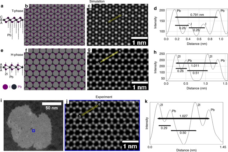
Fig. 2. Atomic resolution ADF-STEM analysis of monolayer 1 H and 1 T phase.
a Side view of the 1 T atomic structure of PbI2. b Top view of the 1 T atomic model of single layer PbI2. c Multislice ADF-STEM image simulation of the 1 T atomic model in b. d Line profile of the lead and iodide intensities marked with yellow line in the atomic model in c, along the direction 1-2. e Side view of 1 H monolayer atomic crystal structure of PbI2. f Top view of the 1 H atomic model of single layer PbI2. g Multislice ADF-STEM image simulation of the 1 H atomic model shown in f. h Line profile of the lead and iodide intensities marked with yellow line in the atomic model in g, along the direction 3–4. i Low-magnification ADF-STEM image of a monolayer PbI2 flake suspended on graphene. j Higher magnification of the region indicated by the blue box in i, showing the 1 H atomic structure. k Line profile taken from region marked by the yellow box in j, which corresponds to same position with the region marked in simulation g, along the direction 5–6.

