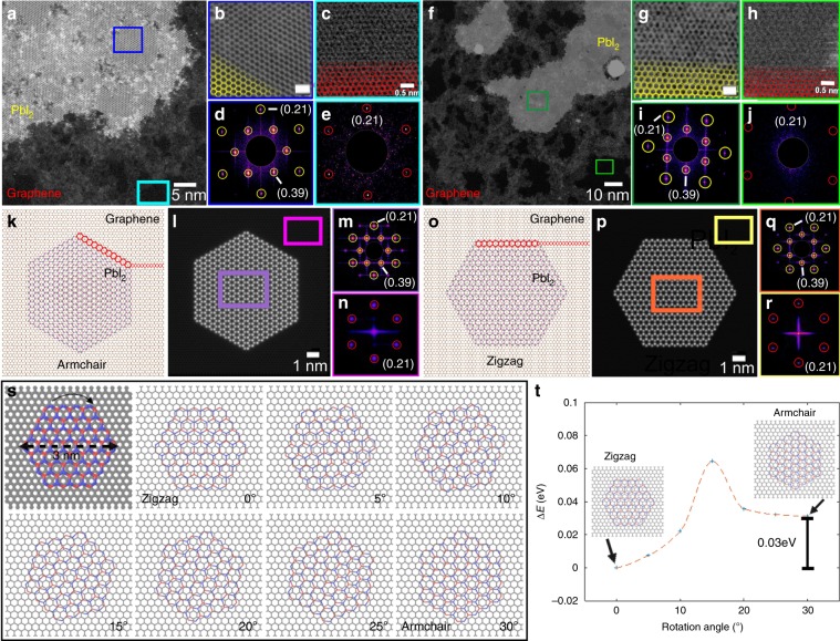
Fig. 3. Crystal orientation of monolayer PbI2 on graphene.
a ADF-STEM images of PbI2 flake suspended on graphene. b High-resolution image of PbI2 crystal annotated in the dark blue box in a. Scale bar corresponds to 1 nm. c High-resolution image of graphene taken from the cyan box region indicated in a. d FFT of PbI2 from the region indicated in b. c FFT of graphene from the region indicated in c. f ADF-STEM images of PbI2 flake suspended on graphene. g High-resolution image of PbI2 crystal indicated by the dark green box in f. Scale bar corresponds to 1 nm. h High-resolution image of graphene from the light green box in f. i FFT of PbI2 from the region indicated in g. h FFT of graphene from the region indicated in f. k Atomic model of PbI2 (1 H) on graphene in the armchair direction. l Multislice image simulations based on the atomic model in k. m FFT of PbI2 from the region indicated by the purple box in l. n FFT of graphene from the region indicated by the pink box in l. o Atomic model of PbI2 (1 H) on graphene in the armchair direction. p Multislice image simulations based on the atomic model in k. q FFT of PbI2 from the region indicated by the orange box in p. r FFT of graphene from the region indicated by the yellow box in p. s Atomic models showing PbI2 relative to graphene for s DFT-relaxed atomic model of PbI2 on graphene, rotated every 5 degrees. t Energy profile of various orientation angles of the PbI2 flake on graphene.

