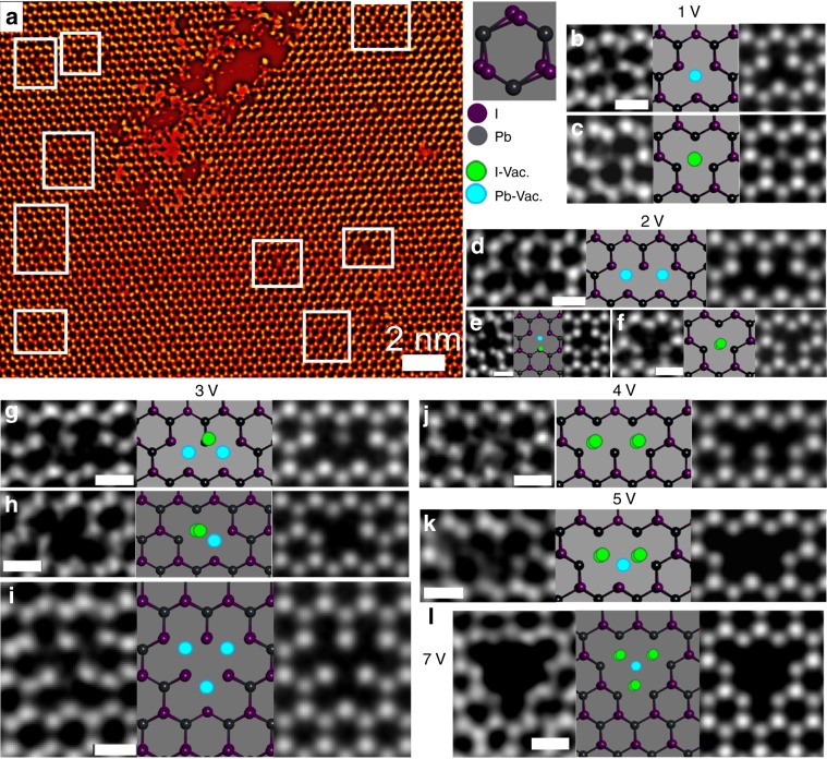
Fig. 5. Vacancy study in monolayer PbI2.
a Low-magnification ADF-STEM image of monolayer PbI2 region after electron beam exposure. The purple and gray spheres correspond to lead and iodide in the structure. The green and blue spheres correspond to the iodide and lead vacancies in the system. ADF-STEM images and their corresponding 1 H PbI2 structured atomic model, as well as multislice simulations have been shown for b point defect with a missing lead atom, c point defect with a missing iodide atom, d double-point defect with two iodide atoms missing, e double-point defect where two lead atoms from adjacent crystal cells are lost, and f double-point defect with one lead and one iodide atoms missing. It can be observed that the single iodide has lower intensity than that of lead or two iodides, g three vacancies formed out of two lead and one iodide loss. It can be observed that the remaining single iodide in the middle has lower intensity than that of lead or two iodides, h three vacancy formed by the absence of three lead atoms from adjacent crystal cells, i another three vacancy formed by two iodide and one lead loss, j four vacancy defect formed by loss of two iodine from adjacent honeycomb structures, k five vacancies formed because of loss of four iodide atoms and a lead atom in a row, l bigger triangular defect formed because of the loss of one lead and six iodide atoms from the center. The scale bar in all the images indicate 0.5 nm.

