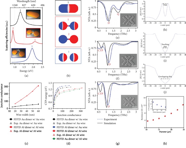
Figure 1.
(a) Numerically computed scattering efficiencies of a single dimer (blue), a conductive nanowire-linked dimer (red), and a nanorod (black). The insets show the schematics of the studied nanostructures. The diameter of the disk is 95 nm, the width and the length of junction wire in the junction are 15 and 30 nm, and the thickness of all structures is 35 nm. (b) Charge plots at the position of scattering peaks for the structures in (a): a dipolar plasmon for the nanorod, capacitively coupled superradiant dipolar resonance (1) and CTP resonance (2) for the nanowire-bridged dimer, and a CTP resonance for the dimer. (c) Experimentally and numerically obtained junction conductances of nanowire-bridged dimers at CTP resonances as a function of nanowire width for aluminum and gold nanostructures. (d) CTP resonance as a function of the junction conductance for nanowire-bridged dimers with varying junction substances [32]. Copyright 2016, American Chemical Society. Characterized and simulated normalized transmission spectra for the metallic assembly for the presence of (e) a nanodisk between gaps, (f) a touching disk to the V-shaped resonators, and (g) an overlapping disk. Insets are the corresponding SEM graphs for disk diameter variations. (h–j) Cross-sectional E-field concentration (∣E∣) diagrams for the presence of a nontouching disk, presence of a touching disk, and presence of an overlapping disk in the middle of the unit cell, respectively. (k) Junction resistance variations as a function of the intermediate disk diameter. Inset is the CTP position as a function of conductive disk diameter [33]. Copyright 2016, Optical Society of America.

