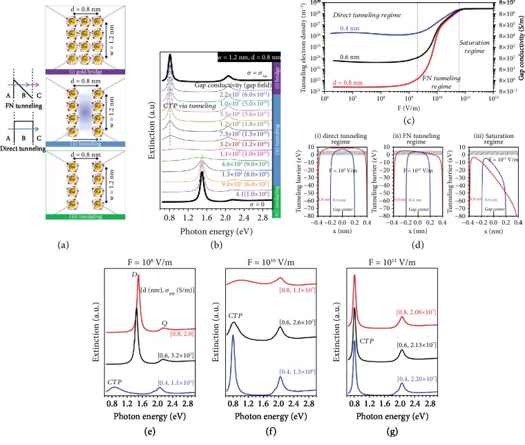
Figure 2.
(a) Schematics of considered regions as conductive gold (the charge transfer track consists of free electrons and gold atoms), conductive gap (the charge transfer path is dominated by either direct or FN tunneling electrons), and insulating gap (the charge transfer route is empty). (b) The simulated extinction spectra of these three regions for a possible range of gap conductivities. (c) The calculated gap conductivity and tunneling electron density as a function of the intensity of the applied electric field for three different gap sizes: 0.8 nm, 0.6 nm, and 0.4 nm. (d) The tunneling barrier profiles within the gap for three possible regimes: (i) direct tunneling, (ii) FN tunneling, and (iii) saturation. In all regimes, the shaded areas indicate the energy levels of the tunneling electrons. (e–g) The simulated extinction spectra for diverse compositions of gap lengths and fields. For the weak field condition in (e), 0.6 nm and 0.8 nm gap sizes could not support the CTP mode, but they can underpin hybridized dipolar (D) and quadrupolar (Q) modes [39]. Copyright 2012, American Chemical Society.

