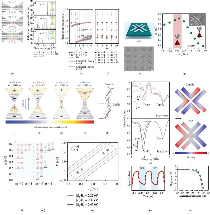
Figure 4.
(a) Details of the junction region in the graphene structures, with definitions of junction length n and width m. (b–d) Computed spectra for particular bridge widths m = 0, 4, and 8 and several other lengths as indicated by different colors. The insets show the complete graphene structures for n = 2. (e) Exhibited plasmon resonances from the graphene structure as a function of bridge width m. The color code for different lengths n is given in the upper inset. The area of the circles is proportional to the area under the extinction peak for each plasmon feature. Conventional plasmon energies are indicated using dashed curves for n = 4 (red) and n = 8 (blue), bordered by shaded areas, representing the strength of the modes. (f) Plasmon resonances as a function of junction length n. The graphene is doped to a Fermi energy EF = 0.4 eV and has a mobility μ = 10,000 cm2/V·s, and the length of the bowties is 8 nm. (g, h, i, j) Charge density maps with the color of each atom indicating its induced charge for different junction widths m = 0, 2, 6, and 8 and the same length n = 4. (k) Induced charge integrated along the horizontal direction and averaged over four nearest carbon-atom neighbors. (l, m) Electron density distribution of electronic states in n = 4 bowtie structures for m = 0 ((l), separated triangles) and m = 6 ((m), linked triangles). The energies of these states are shown by black lines under the density plots. (n) Dipole matrix elements between electronic states of the same bowtie as in (m). The area of the circles is proportional to the dipole strength [77]. Copyright 2013, WILEY-VCH. (o) Schematic of the graphene island-mediated THz cluster. (p) SEM image of the fabricated device. The scale bar is 10 μm. (q) Resistance variations of the graphene monolayer, obtained numerically from the source-drain current with VSD = 25 mV. The inset is the magnified SEM image for the fabricated sample to introduce the geometrical parts as follows: a/b/c/d = 3.5/10/7.5/4 μm. The thickness of the metallic blocks is set to 200 nm, and the scale bar is 5 μm. (r) Normalized transmission amplitude of the graphene-plasmonic structure under applied gate voltage. (s) The current density maps at the dipole and CTP resonance frequencies for the graphene monolayer in dielectric (Vbg = 11 V) and conductive (Vbg = 0 V) regimes. (t) The responding optical signal of the tunable device under fast on/off THz radiation modulation. (u) Experimentally (circles) and numerically (solid line) determined normalized modulation magnitude (dB) [46]. Copyright 2019, Royal Society of Chemistry.

