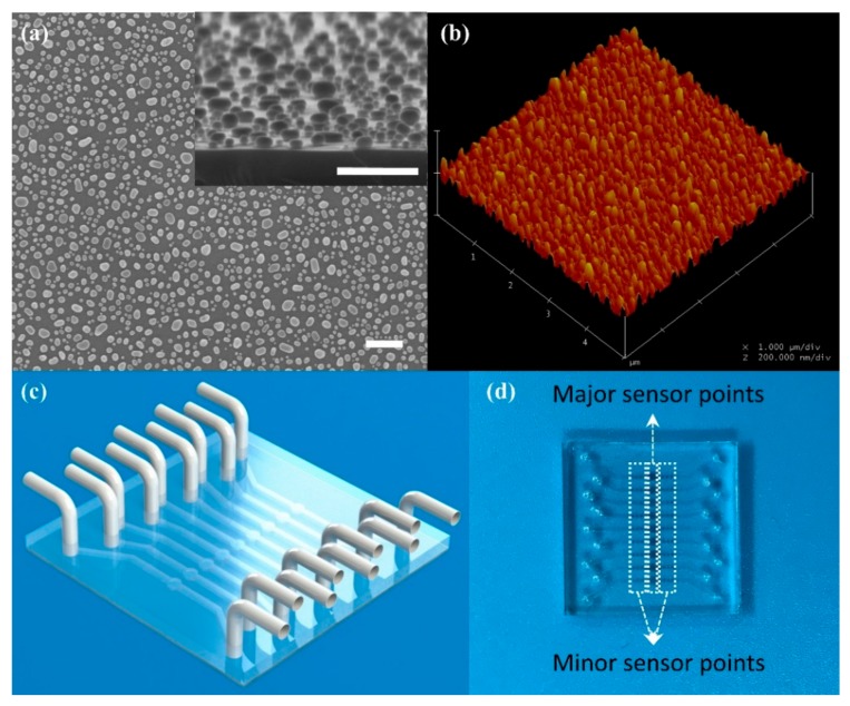
Figure 1.
Schematic of the chip integrated with the microfluidic channel and picture of AuNPs. (a) The SEM (scanning electron microscope) image of AuNPs on a silicon substrate. Insert Figure: side view of AuNPs on a silicon substrate. Scale bar: 300 nm; (b) The AFM (atomic force microscope) image of AuNPs; (c) Schematic of the microfluidic chip; (d) The real picture of the chip.

