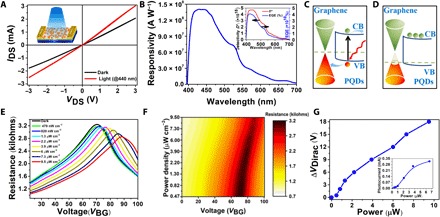
Fig. 3. G-PQD phototransistor.

(A) Drain current (IDS) versus drain voltage (VDS) characteristic of the phototransistor under the dark and illumination intensity of 440 nm monochromatic light with zero gate voltage. Inset: Schematic of G-PQD superstructure phototransistor. (B) Spectral responsivity of G-PQD superstructure phototransistor. Inset: Detectivity and EQE of phototransistor under different wavelengths. Energy level diagram of the G-PQD superstructure under (C) photoexcitation and (D) photogating. VB and CB represent the valence band and conduction band of the PQDs. (E) Resistance as a function of back-gate voltage (VBG) under different illumination intensities at a given drain-source voltage VDS of 500 mV. (F) Two-dimensional plot of superstructure resistance as a function of optical power. (G) Shift of Dirac point as a function of incident light intensity. Inset: Variation of photocurrent under different illumination powers at 437 nm.
