Figure 1:
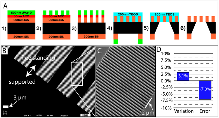
Panel A): Pictographic representation (not to scale) of process workflow steps for the 0.2 μm MSN membrane: 1) deposition of SiN onto double side-polished Si wafers, followed by anti-reflective coating (ARC) and deep UV (DUV) positive photoresist onto the wafers’ frontside (i.e., membrane-side); 2) photolithographic patterning by exposure of DUV photoresist; 3) transfer of slit features into the ARC (via Ar/O2 plasma etching) and transfer into SiN (via reactive ion etching (RIE) with SF6 and He); 4) deposition of protective SiO2 layer (using tetra-orthoethylsilicate [TEOS]) over the transferred slit features, followed by processing on the wafers’ backside to define the freestanding area and outer chip dimensions; 5) bulk through-wafer wet chemical etching; and 6) removal of the protective SiO2 layer to form the final membrane chips with freestanding membranes.
Panel B): Scanning electron micrograph (2,060× magnification; 20 kV) of the resultant freestanding 0.2 μm MSN membranes.
Panel C): Higher magnification micrograph of a portion of the image from panel B).
Panel D): Analysis of variability between achieved and targeted slit width for 0.2 μm MSN membranes.

